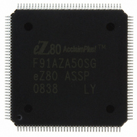
EZ80F91AZA50SG Zilog, EZ80F91AZA50SG Datasheet - Page 235

EZ80F91AZA50SG
Manufacturer Part Number
EZ80F91AZA50SG
Description
IC ACCLAIM MCU 256KB 144LQFP
Manufacturer
Zilog
Series
eZ80® AcclaimPlus!™r
Datasheet
1.EZ80F91AZA50SG.pdf
(387 pages)
Specifications of EZ80F91AZA50SG
Core Processor
Z8
Core Size
8-Bit
Speed
50MHz
Connectivity
Ethernet, I²C, IrDA, SPI, UART/USART
Peripherals
Brown-out Detect/Reset, POR, PWM, WDT
Number Of I /o
32
Program Memory Size
256KB (256K x 8)
Program Memory Type
FLASH
Ram Size
16K x 8
Voltage - Supply (vcc/vdd)
3 V ~ 3.6 V
Oscillator Type
Internal
Operating Temperature
0°C ~ 70°C
Package / Case
144-LQFP
Processor Series
EZ80F91x
Core
eZ80
Data Bus Width
8 bit
Data Ram Size
16 KB
Interface Type
I2C, IrDA, SPI
Maximum Clock Frequency
50 MHz
Number Of Programmable I/os
32
Number Of Timers
4
Operating Supply Voltage
3 V to 3.6 V
Maximum Operating Temperature
+ 70 C
Mounting Style
SMD/SMT
Development Tools By Supplier
eZ80F910300ZCOG
Minimum Operating Temperature
0 C
For Use With
269-4712 - KIT DEV ENCORE 32 SERIES269-4671 - BOARD ZDOTS SBC Z80ACCLAIM PLUS269-4561 - KIT DEV FOR EZ80F91 W/C-COMPILER269-4560 - KIT DEV FOR EZ80F91 W/C-COMPILER
Lead Free Status / RoHS Status
Lead free / RoHS Compliant
Eeprom Size
-
Data Converters
-
Lead Free Status / Rohs Status
Details
Other names
269-4564
Available stocks
Company
Part Number
Manufacturer
Quantity
Price
- Current page: 235 of 387
- Download datasheet (5Mb)
Table 126. I
PS027001-0707
Bit
Position
[7:0]
SLAX
Bit
Reset
CPU Access
Note: R/W = Read/Write.
Bit
Position
[7:0]
DATA
2
C Data Register
I
This register contains the data byte/slave address to be transmitted or the data byte just
received. In TRANSMIT mode, the most-significant bit of the byte is transmitted first. In
RECEIVE mode, the first bit received is placed in the most-significant bit of the register.
After each byte is transmitted, the I
bus in case a lost arbitration event occurs. See
I
The I
master slave relationships on the I
When the Interrupt Enable bit (IEN) is set to 1, the interrupt line goes High when the IFLG
is set to 1. When IEN is cleared to 0, the interrupt line always remains Low.
When the Bus Enable bit (ENAB) is set to 0, the I
ignored and the I
set to 1, the I
GCE bit (I
When the Master Mode Start bit (STA) is set to 1, the I
sends a START condition on the bus when the bus is free. If the STA bit is set to 1 when
the I
repeated START condition is sent. If the STA bit is set to 1 when the I
accessed in SLAVE mode, the I
2
2
C Data Register
C Control Register
Value
00h–FFh Least-significant 8 bits of the 10-bit extended slave address
Value Description
00h–
FFh
2
2
C module is already in MASTER mode and one or more bytes are transmitted, then a
C_CTL register is a control register that is used to control the interrupts and the
R/W
2
I
C_SAR[0]) is set to 1.
7
0
2
C data byte
2
Description
C responds to calls to its slave address and to the general call address if the
2
(I2C_DR = 00CAh)
C module does not respond to any address on the bus. When ENAB is
R/W
6
0
R/W
5
0
2
C completes the data transfer in SLAVE mode and then
2
R/W
C bus.
2
C_DR register contains the byte that is present on the
4
0
R/W
3
0
Table
2
C bus inputs SCLx and SDAx are
R/W
2
0
126.
2
C enters MASTER mode and
R/W
1
0
Product Specification
R/W
0
0
I
2
2
C block is being
C Serial I/O Interface
eZ80F91 ASSP
227
Related parts for EZ80F91AZA50SG
Image
Part Number
Description
Manufacturer
Datasheet
Request
R

Part Number:
Description:
Communication Controllers, ZILOG INTELLIGENT PERIPHERAL CONTROLLER (ZIP)
Manufacturer:
Zilog, Inc.
Datasheet:

Part Number:
Description:
KIT DEV FOR Z8 ENCORE 16K TO 64K
Manufacturer:
Zilog
Datasheet:

Part Number:
Description:
KIT DEV Z8 ENCORE XP 28-PIN
Manufacturer:
Zilog
Datasheet:

Part Number:
Description:
DEV KIT FOR Z8 ENCORE 8K/4K
Manufacturer:
Zilog
Datasheet:

Part Number:
Description:
KIT DEV Z8 ENCORE XP 28-PIN
Manufacturer:
Zilog
Datasheet:

Part Number:
Description:
DEV KIT FOR Z8 ENCORE 4K TO 8K
Manufacturer:
Zilog
Datasheet:

Part Number:
Description:
CMOS Z8 microcontroller. ROM 16 Kbytes, RAM 256 bytes, speed 16 MHz, 32 lines I/O, 3.0V to 5.5V
Manufacturer:
Zilog, Inc.
Datasheet:

Part Number:
Description:
Low-cost microcontroller. 512 bytes ROM, 61 bytes RAM, 8 MHz
Manufacturer:
Zilog, Inc.
Datasheet:

Part Number:
Description:
Z8 4K OTP Microcontroller
Manufacturer:
Zilog, Inc.
Datasheet:

Part Number:
Description:
CMOS SUPER8 ROMLESS MCU
Manufacturer:
Zilog, Inc.
Datasheet:

Part Number:
Description:
SL1866 CMOSZ8 OTP Microcontroller
Manufacturer:
Zilog, Inc.
Datasheet:

Part Number:
Description:
SL1866 CMOSZ8 OTP Microcontroller
Manufacturer:
Zilog, Inc.
Datasheet:

Part Number:
Description:
OTP (KB) = 1, RAM = 125, Speed = 12, I/O = 14, 8-bit Timers = 2, Comm Interfaces Other Features = Por, LV Protect, Voltage = 4.5-5.5V
Manufacturer:
Zilog, Inc.
Datasheet:

Part Number:
Description:
Manufacturer:
Zilog, Inc.
Datasheet:


