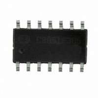
C8051F305-GS Silicon Laboratories Inc, C8051F305-GS Datasheet - Page 83

C8051F305-GS
Manufacturer Part Number
C8051F305-GS
Description
IC 8051 MCU 2K FLASH 14-SOIC
Manufacturer
Silicon Laboratories Inc
Series
C8051F30xr
Specifications of C8051F305-GS
Program Memory Type
FLASH
Program Memory Size
2KB (2K x 8)
Package / Case
14-SOIC (3.9mm Width), 14-SOL
Core Processor
8051
Core Size
8-Bit
Speed
25MHz
Connectivity
SMBus (2-Wire/I²C), UART/USART
Peripherals
POR, PWM, WDT
Number Of I /o
8
Ram Size
256 x 8
Voltage - Supply (vcc/vdd)
2.7 V ~ 3.6 V
Oscillator Type
External
Operating Temperature
-40°C ~ 85°C
Processor Series
C8051F3x
Core
8051
Data Bus Width
8 bit
Data Ram Size
256 B
Interface Type
I2C/SMBus/UART
Maximum Clock Frequency
25 MHz
Number Of Programmable I/os
8
Number Of Timers
3
Maximum Operating Temperature
+ 85 C
Mounting Style
SMD/SMT
3rd Party Development Tools
PK51, CA51, A51, ULINK2
Development Tools By Supplier
C8051F300DK
Minimum Operating Temperature
- 40 C
Lead Free Status / RoHS Status
Lead free / RoHS Compliant
For Use With
770-1006 - ISP 4PORT FOR SILABS C8051F MCU336-1444 - ADAPTER PROGRAM TOOLSTICK F300
Eeprom Size
-
Data Converters
-
Lead Free Status / Rohs Status
Lead free / RoHS Compliant
Other names
336-1540-5
- Current page: 83 of 178
- Download datasheet (2Mb)
9.
Reset circuitry allows the controller to be easily placed in a predefined default condition. On entry to this
reset state, the following occur:
•
•
•
•
All SFRs are reset to the predefined values noted in the SFR detailed descriptions. The contents of internal
data memory are unaffected during a reset; any previously stored data is preserved. However, since the
stack pointer SFR is reset, the stack is effectively lost even though the data on the stack is not altered.
The Port I/O latches are reset to 0xFF (all logic ones) in open-drain mode. Weak pullups are enabled dur-
ing and after the reset. For V
exits the reset state.
On exit from the reset state, the program counter (PC) is reset, and the system clock defaults to the inter-
nal oscillator. Refer to
the system clock source. The Watchdog Timer is enabled with the system clock divided by 12 as its clock
source
Once the system clock source is stable, program execution begins at location 0x0000.
XTAL1
XTAL2
CIP-51 halts program execution
Special Function Registers (SFRs) are initialized to their defined reset values
External Port pins are forced to a known state
Interrupts and timers are disabled.
Reset Sources
(Section “16.3. Watchdog Timer Mode” on page 164
Oscillator
Oscillator
External
Internal
Drive
P0.x
P0.y
Section “11. Oscillators” on page 97
Clock Select
System
Clock
DD
Monitor and power-on resets, the RST pin is driven low until the device
Comparator 0
Figure 9.1. Reset Sources
+
-
Detector
Missing
Clock
(one-
shot)
Microcontroller
EN
Extended Interrupt
C0RSEF
CIP-51
Core
Handler
VDD
WDT
PCA
EN
Rev. 2.9
Supply
Monitor
+
-
System Reset
Enable
Power On
for information on selecting and configuring
Reset
C8051F300/1/2/3/4/5
details the use of the Watchdog Timer).
(Software Reset)
SWRSF
'0'
Operation
FLASH
Illegal
(wired-OR)
Reset
Funnel
/RST
83
Related parts for C8051F305-GS
Image
Part Number
Description
Manufacturer
Datasheet
Request
R
Part Number:
Description:
SMD/C°/SINGLE-ENDED OUTPUT SILICON OSCILLATOR
Manufacturer:
Silicon Laboratories Inc
Part Number:
Description:
Manufacturer:
Silicon Laboratories Inc
Datasheet:
Part Number:
Description:
N/A N/A/SI4010 AES KEYFOB DEMO WITH LCD RX
Manufacturer:
Silicon Laboratories Inc
Datasheet:
Part Number:
Description:
N/A N/A/SI4010 SIMPLIFIED KEY FOB DEMO WITH LED RX
Manufacturer:
Silicon Laboratories Inc
Datasheet:
Part Number:
Description:
N/A/-40 TO 85 OC/EZLINK MODULE; F930/4432 HIGH BAND (REV E/B1)
Manufacturer:
Silicon Laboratories Inc
Part Number:
Description:
EZLink Module; F930/4432 Low Band (rev e/B1)
Manufacturer:
Silicon Laboratories Inc
Part Number:
Description:
I°/4460 10 DBM RADIO TEST CARD 434 MHZ
Manufacturer:
Silicon Laboratories Inc
Part Number:
Description:
I°/4461 14 DBM RADIO TEST CARD 868 MHZ
Manufacturer:
Silicon Laboratories Inc
Part Number:
Description:
I°/4463 20 DBM RFSWITCH RADIO TEST CARD 460 MHZ
Manufacturer:
Silicon Laboratories Inc
Part Number:
Description:
I°/4463 20 DBM RADIO TEST CARD 868 MHZ
Manufacturer:
Silicon Laboratories Inc
Part Number:
Description:
I°/4463 27 DBM RADIO TEST CARD 868 MHZ
Manufacturer:
Silicon Laboratories Inc
Part Number:
Description:
I°/4463 SKYWORKS 30 DBM RADIO TEST CARD 915 MHZ
Manufacturer:
Silicon Laboratories Inc
Part Number:
Description:
N/A N/A/-40 TO 85 OC/4463 RFMD 30 DBM RADIO TEST CARD 915 MHZ
Manufacturer:
Silicon Laboratories Inc
Part Number:
Description:
I°/4463 20 DBM RADIO TEST CARD 169 MHZ
Manufacturer:
Silicon Laboratories Inc


