MC9S08SH4CTJ Freescale Semiconductor, MC9S08SH4CTJ Datasheet - Page 3
MC9S08SH4CTJ
Manufacturer Part Number
MC9S08SH4CTJ
Description
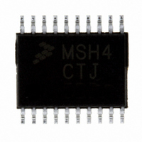
IC MCU 8BIT 4K FLASH 20-TSSOP
Manufacturer
Freescale Semiconductor
Series
HCS08r
Datasheet
1.MC9S08SH4CTJ.pdf
(338 pages)
Specifications of MC9S08SH4CTJ
Core Processor
HCS08
Core Size
8-Bit
Speed
40MHz
Connectivity
I²C, LIN, SCI, SPI
Peripherals
LVD, POR, PWM, WDT
Number Of I /o
17
Program Memory Size
4KB (4K x 8)
Program Memory Type
FLASH
Ram Size
256 x 8
Voltage - Supply (vcc/vdd)
2.7 V ~ 5.5 V
Data Converters
A/D 12x10b
Oscillator Type
Internal
Operating Temperature
-40°C ~ 85°C
Package / Case
20-TSSOP
Processor Series
S08SH
Core
HCS08
Data Bus Width
8 bit
Data Ram Size
256 B
Interface Type
SCI/SPI
Maximum Clock Frequency
40 MHz
Number Of Programmable I/os
17
Number Of Timers
3
Operating Supply Voltage
2.7 V to 5.5 V
Maximum Operating Temperature
+ 85 C
Mounting Style
SMD/SMT
3rd Party Development Tools
EWS08
Development Tools By Supplier
DEMO9S08SG32, DEMO9S08SG32AUTO, DEMO9S08SG8, DEMO9S08SG8AUTO, DEMO9S08SH32, DEMO9S08SH8
Minimum Operating Temperature
- 40 C
On-chip Adc
12-ch x 10-bit
A/d Bit Size
10 bit
A/d Channels Available
12
Height
1.05 mm
Length
6.6 mm
Supply Voltage (max)
5.5 V
Supply Voltage (min)
2.7 V
Width
4.5 mm
Lead Free Status / RoHS Status
Lead free / RoHS Compliant
Eeprom Size
-
Lead Free Status / Rohs Status
Lead free / RoHS Compliant
Available stocks
Company
Part Number
Manufacturer
Quantity
Price

Part Number:
MC9S08SH4CTJR
Manufacturer:
FREESCALE
Quantity:
20 000


MC9S08SH8 Features
8-Bit HCS08 Central Processor Unit (CPU)
On-Chip Memory
Power-Saving Modes
Clock Source Options
System Protection
Development Support
• 40-MHz HCS08 CPU (central processor unit)
• HC08 instruction set with added BGND instruction
• Support for up to 32 interrupt/reset sources
• FLASH read/program/erase over full operating
• Random-access memory (RAM)
• Two very low power stop modes
• Reduced power wait mode
• Very low power real time interrupt for use in run,
• Oscillator (XOSC) — Loop-control Pierce
• Internal Clock Source (ICS) — Internal clock
• Watchdog computer operating properly (COP)
• Low-voltage detection with reset or interrupt;
• Illegal opcode detection with reset
• Illegal address detection with reset
• FLASH block protect
• Single-wire background debug interface
• Breakpoint capability to allow single breakpoint
• On-chip, in-circuit emulation (ICE) debug module
voltage and temperature
wait, and stop
oscillator; Crystal or ceramic resonator range of
31.25 kHz to 38.4 kHz or 1 MHz to 16 MHz
source module containing a frequency-locked
loop (FLL) controlled by internal or external
reference; precision trimming of internal reference
allows 0.2% resolution and 2% deviation over
temperature and voltage; supports bus
frequencies from 2 MHz to 20 MHz.
reset with opti/n to run from dedicated 1-kHz
internal clock source or bus clock
selectable trip points
setting during in-circuit debugging (pluss two
more breakpoints in on-chip debug module)
containing two comparators and nine trigger
modes. Eight deep FIFO for storing
change-of-flow address and event-only data.
Debug module supports both tag and force
breakpoints.
Peripherals
Input/Output
Package Options
• ADC — 12-channel, 10-bit resolution, 2.5 μs
• ACMP — Analog comparator with selectable
• SCI — Full duplex non-return to zero (NRZ); LIN
• SPI — Full-duplex or single-wire bidirectional;
• IIC — Up to 100 kbps with maximum bus loading;
• MTIM — 8-bit modulo counter with 8-bit prescaler
• TPMx — Two 2-channel timer pwm modules
• RTC — (Real-time counter) 8-bit modulus counter
• 17 general purpose I/O pins (GPIOs) and 1
• 8 interrupt pins with selectable polarity
• Ganged output option for PTB[5:2] and PTC[3:0];
• Hysteresis and configurable pull up device on all
• 24-QFN, 20-TSSOP, 20-SOIC, 20-PDIP,
conversion time, automatic compare function,
temperature sensor, internal bandgap reference
channel; runs in stop3
interrupt on rising, falling, or either edge of
comparator output; compare option to fixed
internal bandgap reference voltage; output can be
optionally routed to TPM module; runs in stop3
master extended break generation; LIN slave
extended break detection; wake up on active edge
Double-buffered transmit and receive; Master or
Slave mode; MSB-first or LSB-first shifting
Multi-master operation; Programmable slave
address; Interrupt driven byte-by-byte data
transfer; supports broadcast mode and 10-bit
addressing
and overflow interrupt
(TPM1, TPM2); Selectable input capture, output
compare, or buffered edge- or center-aligned
PWM on each channel
with binary or decimal based prescaler; External
clock source for precise time base, time-of-day,
calendar or task scheduling functions; Free
running on-chip low power oscillator (1 kHz) for
cyclic wake-up without external components, runs
in all MCU modes
output-only pin
allows single write to change state of multiple pins
input pins; Configurable slew rate and drive
strength on all output pins.
16-TSSOP, 8-SOIC
Related parts for MC9S08SH4CTJ
Image
Part Number
Description
Manufacturer
Datasheet
Request
R

Part Number:
Description:
Manufacturer:
Freescale Semiconductor, Inc
Datasheet:
Part Number:
Description:
Manufacturer:
Freescale Semiconductor, Inc
Datasheet:
Part Number:
Description:
Manufacturer:
Freescale Semiconductor, Inc
Datasheet:
Part Number:
Description:
Manufacturer:
Freescale Semiconductor, Inc
Datasheet:
Part Number:
Description:
Manufacturer:
Freescale Semiconductor, Inc
Datasheet:
Part Number:
Description:
Manufacturer:
Freescale Semiconductor, Inc
Datasheet:
Part Number:
Description:
Manufacturer:
Freescale Semiconductor, Inc
Datasheet:
Part Number:
Description:
Manufacturer:
Freescale Semiconductor, Inc
Datasheet:
Part Number:
Description:
Manufacturer:
Freescale Semiconductor, Inc
Datasheet:
Part Number:
Description:
Manufacturer:
Freescale Semiconductor, Inc
Datasheet:
Part Number:
Description:
Manufacturer:
Freescale Semiconductor, Inc
Datasheet:
Part Number:
Description:
Manufacturer:
Freescale Semiconductor, Inc
Datasheet:
Part Number:
Description:
Manufacturer:
Freescale Semiconductor, Inc
Datasheet:
Part Number:
Description:
Manufacturer:
Freescale Semiconductor, Inc
Datasheet:
Part Number:
Description:
Manufacturer:
Freescale Semiconductor, Inc
Datasheet: