C8051F301-GS Silicon Laboratories Inc, C8051F301-GS Datasheet - Page 41
C8051F301-GS
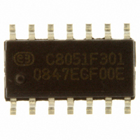
Manufacturer Part Number
C8051F301-GS
Description
IC 8051 MCU 8K FLASH 14-SOIC
Manufacturer
Silicon Laboratories Inc
Series
C8051F30xr
Specifications of C8051F301-GS
Program Memory Type
FLASH
Program Memory Size
8KB (8K x 8)
Package / Case
14-SOIC (3.9mm Width), 14-SOL
Core Processor
8051
Core Size
8-Bit
Speed
25MHz
Connectivity
SMBus (2-Wire/I²C), UART/USART
Peripherals
POR, PWM, WDT
Number Of I /o
8
Ram Size
256 x 8
Voltage - Supply (vcc/vdd)
2.7 V ~ 3.6 V
Oscillator Type
Internal
Operating Temperature
-40°C ~ 85°C
Processor Series
C8051F3x
Core
8051
Data Bus Width
8 bit
Data Ram Size
256 B
Interface Type
I2C/SMBus/UART
Maximum Clock Frequency
25 MHz
Number Of Programmable I/os
8
Number Of Timers
3
Maximum Operating Temperature
+ 85 C
Mounting Style
SMD/SMT
3rd Party Development Tools
PK51, CA51, A51, ULINK2
Development Tools By Supplier
C8051F300DK
Minimum Operating Temperature
- 40 C
Package
14SOIC
Device Core
8051
Family Name
C8051F30x
Maximum Speed
25 MHz
Operating Supply Voltage
3.3 V
Lead Free Status / RoHS Status
Lead free / RoHS Compliant
For Use With
770-1006 - ISP 4PORT FOR SILABS C8051F MCU336-1444 - ADAPTER PROGRAM TOOLSTICK F300336-1319 - REFERENCE DESIGN STEPPER MOTOR
Eeprom Size
-
Data Converters
-
Lead Free Status / Rohs Status
Lead free / RoHS Compliant
Other names
336-1536-5


5.3.3. Settling Time Requirements
When the ADC0 input configuration is changed (i.e., a different AMUX0 or PGA selection is made), a mini-
mum tracking time is required before an accurate conversion can be performed. This tracking time is deter-
mined by the AMUX0 resistance, the ADC0 sampling capacitance, any external source resistance, and the
accuracy required for the conversion. Note that in low-power tracking mode, three SAR clocks are used for
tracking at the start of every conversion. For most applications, these three SAR clocks will meet the mini-
mum tracking time requirements.
Figure 5.5 shows the equivalent ADC0 input circuits for both Differential and Single-ended modes. Notice
that the equivalent time constant for both input circuits is the same. The required ADC0 settling time for a
given settling accuracy (SA) may be approximated by Equation 5.1. When measuring the Temperature
Sensor output or V
settling time (track/hold time) requirements.
Where:
SA is the settling accuracy, given as a fraction of an LSB (for example, 0.25 to settle within 1/4 LSB)
t is the required settling time in seconds
R
n is the ADC resolution in bits (8).
TOTAL
is the sum of the AMUX0 resistance and any external source resistance.
P0.x
P0.y
RC
Differential Mode
MUX Select
MUX Select
Input
DD
= R
Equation 5.1. ADC0 Settling Time Requirements
with respect to GND, R
MUX
R
R
Figure 5.5. ADC0 Equivalent Input Circuits
* C
MUX
MUX
SAMPLE
= 5k
= 5k
Note: When the PGA gain is set to 0.5, C
t
=
C
C
ln
SAMPLE
SAMPLE
------ -
SA
2
= 5pF
= 5pF
n
TOTAL
Rev. 2.9
R
TOTAL
reduces to R
C
P0.x
SAMPLE
C8051F300/1/2/3/4/5
Single-Ended Mode
SAMPLE
RC
MUX
MUX Select
Input
= R
= 3pF
. See Table 5.1 for ADC0 minimum
MUX
R
* C
MUX
SAMPLE
= 5k
C
SAMPLE
= 5pF
41
Related parts for C8051F301-GS
Image
Part Number
Description
Manufacturer
Datasheet
Request
R

Part Number:
Description:
SMD/C°/SINGLE-ENDED OUTPUT SILICON OSCILLATOR
Manufacturer:
Silicon Laboratories Inc
Part Number:
Description:
Manufacturer:
Silicon Laboratories Inc
Datasheet:
Part Number:
Description:
N/A N/A/SI4010 AES KEYFOB DEMO WITH LCD RX
Manufacturer:
Silicon Laboratories Inc
Datasheet:
Part Number:
Description:
N/A N/A/SI4010 SIMPLIFIED KEY FOB DEMO WITH LED RX
Manufacturer:
Silicon Laboratories Inc
Datasheet:
Part Number:
Description:
N/A/-40 TO 85 OC/EZLINK MODULE; F930/4432 HIGH BAND (REV E/B1)
Manufacturer:
Silicon Laboratories Inc
Part Number:
Description:
EZLink Module; F930/4432 Low Band (rev e/B1)
Manufacturer:
Silicon Laboratories Inc
Part Number:
Description:
I°/4460 10 DBM RADIO TEST CARD 434 MHZ
Manufacturer:
Silicon Laboratories Inc
Part Number:
Description:
I°/4461 14 DBM RADIO TEST CARD 868 MHZ
Manufacturer:
Silicon Laboratories Inc
Part Number:
Description:
I°/4463 20 DBM RFSWITCH RADIO TEST CARD 460 MHZ
Manufacturer:
Silicon Laboratories Inc
Part Number:
Description:
I°/4463 20 DBM RADIO TEST CARD 868 MHZ
Manufacturer:
Silicon Laboratories Inc
Part Number:
Description:
I°/4463 27 DBM RADIO TEST CARD 868 MHZ
Manufacturer:
Silicon Laboratories Inc
Part Number:
Description:
I°/4463 SKYWORKS 30 DBM RADIO TEST CARD 915 MHZ
Manufacturer:
Silicon Laboratories Inc
Part Number:
Description:
N/A N/A/-40 TO 85 OC/4463 RFMD 30 DBM RADIO TEST CARD 915 MHZ
Manufacturer:
Silicon Laboratories Inc
Part Number:
Description:
I°/4463 20 DBM RADIO TEST CARD 169 MHZ
Manufacturer:
Silicon Laboratories Inc