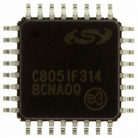
C8051F314-GQ Silicon Laboratories Inc, C8051F314-GQ Datasheet - Page 135

C8051F314-GQ
Manufacturer Part Number
C8051F314-GQ
Description
IC 8051 MCU 8K FLASH 32LQFP
Manufacturer
Silicon Laboratories Inc
Series
C8051F31xr
Specifications of C8051F314-GQ
Program Memory Type
FLASH
Program Memory Size
8KB (8K x 8)
Package / Case
32-LQFP
Core Processor
8051
Core Size
8-Bit
Speed
25MHz
Connectivity
SMBus (2-Wire/I²C), SPI, UART/USART
Peripherals
POR, PWM, WDT
Number Of I /o
29
Ram Size
1.25K x 8
Voltage - Supply (vcc/vdd)
2.7 V ~ 3.6 V
Oscillator Type
Internal
Operating Temperature
-40°C ~ 85°C
Processor Series
C8051F3x
Core
8051
Data Bus Width
8 bit
Data Ram Size
1.25 KB
Interface Type
I2C/SMBus/SPI/UART
Maximum Clock Frequency
25 MHz
Number Of Programmable I/os
29
Number Of Timers
4
Operating Supply Voltage
2.7 V to 3.6 V
Maximum Operating Temperature
+ 85 C
Mounting Style
SMD/SMT
3rd Party Development Tools
PK51, CA51, A51, ULINK2
Development Tools By Supplier
C8051F310DK
Minimum Operating Temperature
- 40 C
On-chip Adc
17-chx10-bit
No. Of I/o's
29
Ram Memory Size
1280Byte
Cpu Speed
25MHz
No. Of Timers
4
Rohs Compliant
Yes
Lead Free Status / RoHS Status
Lead free / RoHS Compliant
For Use With
770-1006 - ISP 4PORT FOR SILABS C8051F MCU336-1445 - ADAPTER PROGRAM TOOLSTICK F310
Eeprom Size
-
Data Converters
-
Lead Free Status / Rohs Status
Lead free / RoHS Compliant
Other names
336-1257
Available stocks
Company
Part Number
Manufacturer
Quantity
Price
Company:
Part Number:
C8051F314-GQ
Manufacturer:
Silicon Laboratories Inc
Quantity:
10 000
Company:
Part Number:
C8051F314-GQR
Manufacturer:
ST
Quantity:
15 000
Company:
Part Number:
C8051F314-GQR
Manufacturer:
Silicon Laboratories Inc
Quantity:
10 000
13.3. General Purpose Port I/O
Port pins that remain unassigned by the Crossbar and are not used by analog peripherals can be used for
general purpose I/O. Ports3-0 are accessed through corresponding special function registers (SFRs) that
are both byte addressable and bit addressable. When writing to a Port, the value written to the SFR is
latched to maintain the output data value at each pin. When reading, the logic levels of the Port's input pins
are returned regardless of the XBRn settings (i.e., even when the pin is assigned to another signal by the
Crossbar, the Port register can always read its corresponding Port I/O pin). The exception to this is the
execution of the read-modify-write instructions. The read-modify-write instructions when operating on a
Port SFR are the following: ANL, ORL, XRL, JBC, CPL, INC, DEC, DJNZ and MOV, CLR or SET, when the
destination is an individual bit in a Port SFR. For these instructions, the value of the register (not the pin) is
read, modified, and written back to the SFR.
Bit7:
Bit6:
Bit5:
Bit4:
Bit3:
Bits2–0: PCA0ME: PCA Module I/O Enable Bits.
WEAKPUD XBARE
R/W
Bit7
WEAKPUD: Port I/O Weak Pullup Disable.
0: Weak Pullups enabled (except for Ports whose I/O are configured as analog input).
1: Weak Pullups disabled.
XBARE: Crossbar Enable.
0: Crossbar disabled.
1: Crossbar enabled.
T1E: T1 Enable
0: T1 unavailable at Port pin.
1: T1 routed to Port pin.
T0E: T0 Enable
0: T0 unavailable at Port pin.
1: T0 routed to Port pin.
ECIE: PCA0 External Counter Input Enable
0: ECI unavailable at Port pin.
1: ECI routed to Port pin.
000: All PCA I/O unavailable at Port pins.
001: CEX0 routed to Port pin.
010: CEX0, CEX1 routed to Port pins.
011: CEX0, CEX1, CEX2 routed to Port pins.
100: CEX0, CEX1, CEX2, CEX3 routed to Port pins.
101: CEX0, CEX1, CEX2, CEX3, CEX4 routed to Port pins.
SFR Definition 13.2. XBR1: Port I/O Crossbar Register 1
R/W
Bit6
T1E
R/W
Bit5
T0E
R/W
Bit4
Rev. 1.7
ECIE
R/W
Bit3
C8051F310/1/2/3/4/5/6/7
R/W
Bit2
PCA0ME
R/W
Bit1
R/W
Bit0
SFR Address:
00000000
Reset Value
0xE2
135


