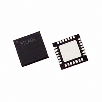
C8051F311-GM Silicon Laboratories Inc, C8051F311-GM Datasheet - Page 216

C8051F311-GM
Manufacturer Part Number
C8051F311-GM
Description
IC 8051 MCU 16K FLASH 28MLP
Manufacturer
Silicon Laboratories Inc
Series
C8051F31xr
Datasheets
1.C8051F310-TB.pdf
(228 pages)
2.C8051F311-GM.pdf
(2 pages)
3.C8051F310-GQ.pdf
(218 pages)
Specifications of C8051F311-GM
Program Memory Type
FLASH
Program Memory Size
16KB (16K x 8)
Package / Case
28-VQFN Exposed Pad, 28-HVQFN, 28-SQFN, 28-DHVQFN
Core Processor
8051
Core Size
8-Bit
Speed
25MHz
Connectivity
SMBus (2-Wire/I²C), SPI, UART/USART
Peripherals
POR, PWM, Temp Sensor, WDT
Number Of I /o
25
Ram Size
1.25K x 8
Voltage - Supply (vcc/vdd)
2.7 V ~ 3.6 V
Data Converters
A/D 17x10b
Oscillator Type
Internal
Operating Temperature
-40°C ~ 85°C
Processor Series
C8051F3x
Core
8051
Data Bus Width
8 bit
Data Ram Size
1.25 KB
Interface Type
I2C, SMBus, SPI, UART
Maximum Clock Frequency
25 MHz
Number Of Programmable I/os
25
Number Of Timers
4 bit
Operating Supply Voltage
2.7 V to 3.6 V
Maximum Operating Temperature
+ 85 C
Mounting Style
SMD/SMT
3rd Party Development Tools
PK51, CA51, A51, ULINK2
Development Tools By Supplier
C8051F310DK
Minimum Operating Temperature
- 40 C
On-chip Adc
10 bit, 17 Channel
No. Of I/o's
25
Ram Memory Size
1280Byte
Cpu Speed
25MHz
No. Of Timers
4
Rohs Compliant
Yes
Package
24QFN EP
Device Core
8051
Family Name
C8051F31x
Maximum Speed
25 MHz
Lead Free Status / RoHS Status
Lead free / RoHS Compliant
For Use With
770-1006 - ISP 4PORT FOR SILABS C8051F MCU336-1446 - ADAPTER PROGRAM TOOLSTICK F311336-1253 - DEV KIT FOR C8051F310/F311
Eeprom Size
-
Lead Free Status / Rohs Status
Lead free / RoHS Compliant
Other names
336-1254
Available stocks
Company
Part Number
Manufacturer
Quantity
Price
Part Number:
C8051F311-GM
Manufacturer:
SILICONLABS/芯科
Quantity:
20 000
Part Number:
C8051F311-GMR
Manufacturer:
SILICON LABS/芯科
Quantity:
20 000
C8051F310/1/2/3/4/5
D
Revision 1.4 to Revision 1.5
•
•
•
•
•
•
•
•
•
•
•
•
•
•
•
•
•
•
•
•
•
•
216
OCUMENT
Added four part numbers: C8051F312, C8051F313, C8051F314, and C8051F315.
Modified all sections to accommodate the four new part numbers.
Removed preliminary tag.
Changed title of Figure 4.6 to "MLP-28 Solder Paste Recommendation."
Added reference to minimum tracking time in Section
Changed bit 6 to read only in “SFR Definition 7.1. CPT0CN: Comparator0 Control” on page 64, and
“SFR Definition 7.4. CPT1CN: Comparator1 Control” on page 67.
In Section
bit should take more than one clock cycle.
In Section
should take more than one clock cycle.
In “SFR Definition 8.4. PSW: Program Status Word” on page 84, clarified OV flag description.
In “SFR Definition 8.8. IP: Interrupt Priority” on page 90, changed "default priority order" to "low prior-
ity" for low priority descriptions.
In Section
In Section
power-on reset.
In Table 9.1, “Reset Electrical Characteristics,” on page 102, added VDD Ramp Time and changed
"VDD POR Threshold" to "VDD Monitor Threshold."
In Section
In “SFR Definition 12.3. CLKSEL: Clock Select” on page 113, and Section
Selection” on page 114, changed reference from CLKSL0 in the OSCICN register to CLKSL0 in the
CLKSEL register.
In Section
and added a specific 32.768 kHz crystal example.
In Figure 13.3 on Page 121 and Figure 13.4 on Page 122 (Crossbar Priority Decoder), added note for
NSS in SPI 3-wire and 4-wire modes and changed PnSKIP[7:0] to PnSKIP[0:7] to match the Port I/O
order.
In “SFR Definition 14.1. SMB0CF: SMBus Clock/Configuration” on page 142, added a description of
the behavior of Timer 3 in split mode if SMBTOE is set.
Throughout Section
and "TMR2H," respectively; and changed references to "TL3" and "TH3" to "TMR3L" and "TMR3H,"
respectively.
In “SFR Definition 17.13. TMR3CN: Timer 3 Control” on page 191, changed to refer to Timer 3 in the
TF3H bit description.
In Section
Changed registers from figures to SFR Definitions and C2 Register Definitions.
“8.3. Interrupt
“8.4.1. Idle
“9.1. Power-On
“9.1. Power-On
“10.3. Security
“12.4. External Crystal
“17.
C
Timers” on page 177, removed incorrect references to the Timer 3 interrupt bit in IE.
HANGE
“17.
Mode” on page 94, added note stating the instruction after setting the IDLE bit
Timers” on page 177, changed references to "TL2" and "TH2" to "TMR2L"
Handler” on page 86, added note stating the instruction after clearing the EA
Options” on page 105, clarified descriptions of Flash security features.
Reset” on page 98, changed description to VDD Monitor is disabled after a
Reset” on page 98, clarified description of VDD Ramp Time.
L
IST
Example” on page 116, clarified external crystal initialization steps
Rev. 1.5
“5.3.2. Tracking
Modes” on page 48.
“12.3. System Clock


