C8051F507-IQ Silicon Laboratories Inc, C8051F507-IQ Datasheet
C8051F507-IQ
Specifications of C8051F507-IQ
Available stocks


Related parts for C8051F507-IQ

C8051F507-IQ Summary of contents
Page 1
Analog Peripherals - 12-Bit ADC Up to 200 ksps • external single-ended inputs • VREF from on-chip VREF, external pin or V • Internal or external start of conversion source • Built-in temperature sensor • - Two ...
Page 2
C8051F50x/F51x 2 Rev. 1.2 ...
Page 3
Table of Contents 1. System Overview ..................................................................................................... 16 2. Ordering Information ............................................................................................... 20 3. Pin Definitions.......................................................................................................... 22 4. Package Specifications ........................................................................................... 30 4.1. QFP-48 Package Specifications........................................................................ 30 4.2. QFN-48 Package Specifications........................................................................ 32 4.3. QFN-40 Package Specifications........................................................................ 34 4.4. QFP-32 Package ...
Page 4
C8051F50x/F51x 12.2.1.3. Stack ............................................................................................ 99 13. Special Function Registers................................................................................. 100 13.1. SFR Paging ................................................................................................... 100 13.2. Interrupts and SFR Paging ............................................................................ 100 13.3. SFR Page Stack Example ............................................................................. 101 14. Interrupts .............................................................................................................. 117 14.1. MCU Interrupt Sources and Vectors.............................................................. 117 ...
Page 5
Memory Mode Selection................................................................................ 155 18.5.1. Internal XRAM Only .............................................................................. 155 18.5.2. Split Mode without Bank Select............................................................. 155 18.5.3. Split Mode with Bank Select.................................................................. 156 18.5.4. External Only......................................................................................... 156 18.6. Timing .......................................................................................................... 156 18.6.1. Non-Multiplexed Mode .......................................................................... 158 18.6.1.1. 16-bit ...
Page 6
C8051F50x/F51x 21.5. Sleep Mode and Wake-Up ............................................................................ 207 21.6. Error Detection and Handling ........................................................................ 207 21.7. LIN Registers................................................................................................. 208 21.7.1. LIN Direct Access SFR Registers Definitions ....................................... 208 21.7.2. LIN Indirect Access SFR Registers Definitions ..................................... 210 22. Controller Area ...
Page 7
Serial Clock (SCK) ................................................................................ 253 25.1.4. Slave Select (NSS) ............................................................................... 253 25.2. SPI0 Master Mode Operation ........................................................................ 254 25.3. SPI0 Slave Mode Operation .......................................................................... 256 25.4. SPI0 Interrupt Sources .................................................................................. 256 25.5. Serial Clock Phase and Polarity .................................................................... 257 ...
Page 8
C8051F50x/F51x List of Figures Figure 1.1. C8051F500/1/4/5 Block Diagram .......................................................... 17 Figure 1.2. C8051F508/9-F510/1 Block Diagram .................................................... 18 Figure 1.3. C8051F502/3/6/7 Block Diagram .......................................................... 19 Figure 3.1. QFP-48 Pinout Diagram (Top View) ...................................................... 25 Figure 3.2. QFN-48 Pinout Diagram (Top ...
Page 9
Figure 13.5. SFR Page Stack Upon Return From PCA Interrupt .......................... 105 Figure 13.6. SFR Page Stack Upon Return From CAN0 Interrupt ........................ 106 Figure 15.1. Flash Program Memory Map ............................................................. 131 Figure 17.1. Reset Sources ................................................................................... 141 Figure 17.2. ...
Page 10
C8051F50x/F51x Figure 25.5. Master Mode Data/Clock Timing ....................................................... 257 Figure 25.6. Slave Mode Data/Clock Timing (CKPHA = 0) ................................... 258 Figure 25.7. Slave Mode Data/Clock Timing (CKPHA = 1) ................................... 258 Figure 25.8. SPI Master Timing (CKPHA = 0) ....................................................... ...
Page 11
List of Tables Table 2.1. Product Selection Guide ......................................................................... 21 Table 3.1. Pin Definitions for the C8051F50x-F51x ................................................. 22 Table 4.1. QFP-48 Package Dimensions ................................................................ 30 Table 4.2. QFP-48 Landing Diagram Dimensions ................................................... 31 Table 4.3. QFN-48 Package Dimensions ................................................................ ...
Page 12
C8051F50x/F51x Table 21.3. Autobaud Parameters Examples ........................................................ 205 Table 21.4. LIN Registers (Indirectly Addressable) ............................................... 210 Table 22.1. Background System Information ........................................................ 220 Table 22.2. Standard CAN Registers and Reset Values ....................................... 223 Table 23.1. SMBus Clock Source Selection .......................................................... ...
Page 13
List of Registers SFR Definition 6.4. ADC0CF: ADC0 Configuration ...................................................... 63 SFR Definition 6.5. ADC0H: ADC0 Data Word MSB .................................................... 64 SFR Definition 6.6. ADC0L: ADC0 Data Word LSB ...................................................... 64 SFR Definition 6.7. ADC0CN: ADC0 Control ................................................................ 65 SFR ...
Page 14
C8051F50x/F51x SFR Definition 17.2. RSTSRC: Reset Source ............................................................ 146 SFR Definition 18.1. EMI0CN: External Memory Interface Control ............................ 151 SFR Definition 18.2. EMI0CF: External Memory Configuration .................................. 152 SFR Definition 18.3. EMI0TC: External Memory Timing Control ................................ 157 SFR Definition ...
Page 15
SFR Definition 23.3. SMB0DAT: SMBus Data ............................................................ 236 SFR Definition 24.1. SCON0: Serial Port 0 Control .................................................... 248 SFR Definition 24.2. SMOD0: Serial Port 0 Control .................................................... 249 SFR Definition 24.3. SBUF0: Serial (UART0) Port Data Buffer .................................. 250 SFR ...
Page 16
C8051F50x/F51x 1. System Overview C8051F50x/F51x devices are fully integrated mixed-signal System-on-a-Chip MCUs. Highlighted features are listed below. Refer to Table 2.1 for specific product feature selection and part ordering numbers. High-speed pipelined 8051-compatible microcontroller core ( MIPS) ...
Page 17
Power On CIP-51 8051 Reset Controller Core Reset up to 64kB Byte Flash Program Memory Debug / C2CK/RST Programming 256 Byte RAM Hardware C2D 4 kB XRAM Voltage Regulator VREGIN (LDO) VDD GND System Clock Setup XTAL1 Internal Oscillator External ...
Page 18
C8051F50x/F51x Power On CIP-51 8051 Reset Controller Core Reset Byte Flash Program Memory C2CK/RST Debug / Programming 256 Byte RAM Hardware 4 kB XRAM C2D Voltage Regulator VREGIN (LDO) VDD GND System Clock Setup XTAL1 Internal ...
Page 19
Power On CIP-51 8051 Reset Controller Core Reset up to 64kB Byte Flash Program Memory Debug / C2CK/RST Programming 256 Byte RAM Hardware 4 kB XRAM C2D Voltage Regulator VREGIN (LDO) VDD GND System Clock Setup XTAL1 XTAL2 Internal Oscillator ...
Page 20
C8051F50x/F51x 2. Ordering Information The following features are common to all devices in this family: 50 MHz system clock and 50 MIPS throughput (peak) 4352 bytes of RAM (256 internal bytes and 4096 XRAM bytes) 2 SMBus/I ...
Page 21
... Please contact Silicon Labs sales for more information regarding –AM and -AQ devices for your automotive project. C8051F50x/F51x QFP-48 C8051F505-IQ 32 QFN-48 C8051F505-IM 32 QFP-48 C8051F506-IQ 32 QFN-48 C8051F506-IM 32 QFP-32 C8051F507-IQ 32 QFN-32 C8051F507-IM 32 QFP-32 C8051F508-IM 64 QFN-32 C8051F509-IM 64 QFP-48 C8051F510-IM 32 QFN-48 C8051F511-IM 32 Rev. 1.2 — — 40 QFP-48 ...
Page 22
C8051F50x/F51x 3. Pin Definitions Table 3.1. Pin Definitions for the C8051F50x/F51x Name Pin Pin ‘F500/1/4/5 F508/9- F510/1 (40-pin) (48-pin) VDD 4 4 GND 6 6 VDDA 5 5 GNDA 7 7 VREGIN 3 3 VIO 2 2 RST ...
Page 23
Table 3.1. Pin Definitions for the C8051F50x/F51x(Continued) Name Pin Pin ‘F500/1/4/5 F508/9- ‘F502/3/6/7 F510/1 (40-pin) (48-pin ...
Page 24
C8051F50x/F51x Table 3.1. Pin Definitions for the C8051F50x/F51x(Continued) Name Pin Pin ‘F500/1/4/5 F508/9- F510/1 (40-pin) (48-pin) P3 P4.0 18 — P4.1 17 — P4.2 16 — P4.3 15 — P4.4 14 — P4.5 13 — P4.6 10 — ...
Page 25
P0.1/CNVSTR 1 VIO 2 VREGIN 3 VDD 4 VDDA 5 GND 6 GNDA 7 P0.0 / VREF 8 P4.7 9 P4.6 10 C2D 11 RST/C2CK 12 Figure 3.1. QFP-48 Pinout Diagram (Top View) C8051F50x/F51x C8051F500-IQ C8051F501-IQ C8051F504-IQ C8051F505-IQ Top View ...
Page 26
C8051F50x/F51x P0.1/CNVSTR 1 VIO 2 VREGIN 3 VDD 4 VDDA 5 GND 6 GNDA 7 P0.0 / VREF 8 P4.7 9 P4.6 10 C2D 11 RST/C2CK 12 Figure 3.2. QFN-48 Pinout Diagram (Top View) 26 C8051F500-IM C8051F501-IM C8051F504-IM C8051F505-IM Top ...
Page 27
P0.1 / CNVSTR 1 VIO 2 VREGIN 3 VDD 4 VDDA 5 GND 6 GNDA 7 P0.0 / VREF 8 P4.0 / C2D 9 RST / C2CK 10 Figure 3.3. QFN-40 Pinout Diagram (Top View) C8051F50x/F51x C8051F508-IM C8051F509-IM C8051F510-IM C8051F511-IM ...
Page 28
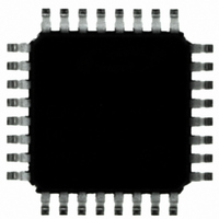
... C8051F50x/F51x 1 P0.1/CNVSTR VIO 2 VREGIN 3 VDD 4 VDDA 5 6 GND 7 GNDA 8 P0.0/VREF Figure 3.4. QFP-32 Pinout Diagram (Top View) 28 C8051F502-IQ C8051F503-IQ C8051F506-IQ C8051F507-IQ Top View Rev. 1.2 24 P1.2 23 P1.3 22 P1.4 21 P1.5 20 P1.6 19 P1.7 18 P2.0 17 P2.1 ...
Page 29
... P0.1/CNVSTR 1 VIO 2 C8051F502-IM VREGIN 3 C8051F503-IM VDD 4 C8051F506-IM VDDA 5 C8051F507-IM GND 6 GNDA 7 P0.0/VREF 8 Figure 3.5. QFN-32 Pinout Diagram (Top View) C8051F50x/F51x Top View 19 18 GND 17 Rev. 1.2 P1.2 P1.3 P1.4 P1.5 P1.6 P1.7 P2.0 P2.1 29 ...
Page 30
C8051F50x/F51x 4. Package Specifications 4.1. QFP-48 Package Specifications Figure 4.1. QFP-48 Package Drawing Table 4.1. QFP-48 Package Dimensions Dimension Min Typ A — — A1 0.05 — A2 0.95 1.00 b 0.17 0.22 c 0.09 — D 9.00 BSC. D1 ...
Page 31
Figure 4.2. QFP-48 Landing Diagram Table 4.2. QFP-48 Landing Diagram Dimensions Dimension Min C1 8.30 C2 8.30 E 0.50 BSC Notes: General 1. All dimensions shown are in millimeters (mm) unless otherwise noted. 2. This Land Pattern Design is based ...
Page 32
C8051F50x/F51x 4.2. QFN-48 Package Specifications Figure 4.3. QFN-48 Package Drawing Table 4.3. QFN-48 Package Dimensions Dimension Min Typ A 0.80 0. 0.18 0.23 D 7.00 BSC D2 3.90 4.00 e 0.50 BSC E 7.00 BSC Notes: ...
Page 33
Figure 4.4. QFN-48 Landing Diagram Table 4.4. QFN-48 Landing Diagram Dimensions Dimension Min C1 6.80 C2 6.80 e 0.50 BSC X1 0.20 Notes: General 1. All dimensions shown are in millimeters (mm) unless otherwise noted. 2. Dimension and Tolerancing is ...
Page 34
C8051F50x/F51x 4.3. QFN-40 Package Specifications Figure 4.5. Typical QFN-40 Package Drawing Table 4.5. QFN-40 Package Dimensions Dimension Min Typ A 0.80 0.85 A1 0.00 b 0.18 0.23 D 6.00 BSC D2 4.00 4.10 e 0.50 BSC E 6.00 BSC Notes: ...
Page 35
Figure 4.6. QFN-40 Landing Diagram Table 4.6. QFN-40 Landing Diagram Dimensions Dimension Min C1 5.80 C2 5.80 e 0.50 BSC X1 0.15 Notes: General 1. All dimensions shown are in millimeters (mm) unless otherwise noted. 2. Dimension and Tolerancing is ...
Page 36
C8051F50x/F51x 4.4. QFP-32 Package Specifications Figure 4.7. QFP-32 Package Drawing Table 4.7. QFP-32 Package Dimensions Dimension Min Typ A — — A1 0.05 — A2 1.35 1.40 b 0.30 0.37 c 0.09 — D 9.00 BSC. D1 7.00 BSC. e ...
Page 37
Figure 4.8. QFP-32 Package Drawing Table 4.8. QFP-32 Landing Diagram Dimensions Dimension Min C1 8.40 C2 8.40 E 0.80 BSC Notes: General 1. All dimensions shown are in millimeters (mm) unless otherwise noted. 2. This Land Pattern Design is based ...
Page 38
C8051F50x/F51x 4.5. QFN-32 Package Specifications Figure 4.9. QFN-32 Package Drawing Table 4.9. QFN-32 Package Dimensions Dimension Min Typ A 0.80 0.9 A1 0.00 0.02 b 0.18 0.25 D 5.00 BSC. D2 3.20 3.30 e 0.50 BSC. E 5.00 BSC. Notes: ...
Page 39
Figure 4.10. QFN-32 Package Drawing Table 4.10. QFN-32 Landing Diagram Dimensions Dimension Min C1 4.80 C2 4.80 e 0.50 BSC X1 0.20 Notes: General 1. All dimensions shown are in millimeters (mm) unless otherwise noted. 2. This Land Pattern Design ...
Page 40
C8051F50x/F51x 5. Electrical Characteristics 5.1. Absolute Maximum Specifications Table 5.1. Absolute Maximum Ratings Parameter Ambient Temperature under Bias Storage Temperature Voltage on V with Respect to GND REGIN Voltage on V with Respect to GND DD Voltage on VDDA with ...
Page 41
Electrical Characteristics Table 5.2. Global Electrical Characteristics –40 to +125 °C, 24 MHz system clock unless otherwise specified. Parameter Supply Input Voltage (V ) REGIN Digital Supply Voltage (V ) System Clock < 25 MHz DD System Clock > ...
Page 42
C8051F50x/F51x Table 5.2. Global Electrical Characteristics (Continued) –40 to +125 °C, 24 MHz system clock unless otherwise specified. Parameter MHz I Supply Sensitivity DD F ...
Page 43
Table 5.2. Global Electrical Characteristics (Continued) –40 to +125 °C, 24 MHz system clock unless otherwise specified. Parameter Digital Supply Current—CPU Inactive (Idle Mode, not fetching instructions from Flash ...
Page 44
C8051F50x/F51x Figure 5.1. Minimum VDD Monitor Threshold vs. System Clock Frequency Note: With system clock frequencies greater than 25 MHz, the VDD monitor level should be set to the high threshold (VDMLVL = 1b in SFR VDM0CN) to prevent undefined ...
Page 45
Table 5.3. Port I/O DC Electrical Characteristics V = 1.8 to 2.75 V, –40 to +125 °C unless otherwise specified. DD Parameters Conditions Output High I = –3 mA, Port I/O push-pull OH Voltage I = –10 µA, Port I/O ...
Page 46
C8051F50x/F51x Table 5.4. Reset Electrical Characteristics –40 to +125 °C unless otherwise specified. Parameter RST Output Low Voltage RST Input High Voltage RST Input Low Voltage RST Input Pullup Current V RST Threshold ( RST-LOW V RST Threshold ...
Page 47
Table 5.6. Internal High-Frequency Oscillator Electrical Characteristics V = 1.8 to 2.75 V, –40 to +125 °C unless otherwise specified; Using factory-calibrated settings. DD Parameter Oscillator Frequency IFCN = 111b; VDD > VREGMIN IFCN = 111b; VDD < VREGMIN Oscillator ...
Page 48
C8051F50x/F51x Table 5.7. Clock Multiplier Electrical Specifications V = 1.8 to 2.75 V, –40 to +125 °C unless otherwise specified. DD Parameter Input Frequency (Fcm ) in Output Frequency Power Supply Current Table 5.8. Voltage Regulator Electrical Characteristics V = ...
Page 49
Table 5.9. ADC0 Electrical Characteristics VDDA = 1.8 to 2.75 V, –40 to +125 °C, VREF = 1.5 V (REFSL=0) unless otherwise specified. Parameter DC Accuracy Resolution Integral Nonlinearity Differential Nonlinearity 1 Offset Error Full Scale Error Offset Temperature Coefficient ...
Page 50
C8051F50x/F51x Table 5.10. Temperature Sensor Electrical Characteristics VDDA = 1.8 to 2.75 V, –40 to +125 °C unless otherwise specified. Parameter Linearity Slope Slope Error* Offset Offset Error* Power Supply Current Tracking Time *Note: Represents one standard deviation from the ...
Page 51
Table 5.12. Comparator 0 and Comparator 1 Electrical Characteristics VIO = 1.8 to 5.125 V, –40 to +125 °C unless otherwise noted. Parameter Response Time: CPn+ – CPn– = 100 mV * Mode 0, Vcm = 1.5 V CPn+ – ...
Page 52
C8051F50x/F51x 6. 12-Bit ADC (ADC0) The ADC0 on the C8051F50x/F51x consists of an analog multiplexer (AMUX0) with 35/28 total input selec- tions and a 200 ksps, 12-bit successive-approximation-register (SAR) ADC with integrated track-and-hold, programmable window detector, programmable attenuation (1:2), and ...
Page 53
Modes of Operation In a typical system, ADC0 is configured using the following steps gain adjustment is required, refer to Section “6.3. Selectable Gain” on page 58. 2. Choose the start of conversion source. 3. Choose ...
Page 54
C8051F50x/F51x Post-Tracking Mode is selected when AD0TM is set to 01b. A programmable tracking time based on AD0TK is started immediately following the convert start signal. Conversions are started after the pro- grammed tracking time ends. After a conversion is ...
Page 55
Convert Start Time F S1 ADC0 State AD0INT Flag Post-Tracking or Dual-Tracking Modes (AD0TK = ‘00') Time F S1 ADC0 State Track AD0INT Flag Key F Sn Figure 6.3. 12-Bit ADC Tracking Mode Example 6.1.4. Burst Mode Burst Mode is ...
Page 56
C8051F50x/F51x been accumulated. Similarly, the Window Comparator will not compare the result to the greater-than and less-than registers until “repeat count” conversions have been accumulated. Note: When using Burst Mode, care must be taken to issue a convert start signal ...
Page 57
Output Code Formatting The registers ADC0H and ADC0L contain the high and low bytes of the output conversion code. When the repeat count is set to 1, conversion codes are represented in 12-bit unsigned integer format and the output ...
Page 58
C8051F50x/F51x Figure 6.5. ADC0 Equivalent Input Circuit 6.3. Selectable Gain ADC0 on the C8051F50x/F51x family of devices implements a selectable ...
Page 59
For example, if ADC0GNH = 0xFC, ADC0GNL = 0x00, and GAINADD = 1, GAIN = 0xFC0 = 4032, and the resulting equation is as follows: 4032 ------------ - GAIN = 4096 The table below equates values in the ...
Page 60
C8051F50x/F51x 6.3.2. Setting the Gain Value The three programmable gain registers are accessed indirectly using the ADC0H and ADC0L registers when the GAINEN bit (ADC0CF.0) bit is set. ADC0H acts as the address register, and ADC0L is the data register. ...
Page 61
Gain Register Definition 6.1. ADC0GNH: ADC0 Selectable Gain High Byte Bit 7 6 Name Type 1 1 Reset Indirect Address = 0x04; Bit Name 7:0 GAINH[7:0] ADC0 Gain High Byte. See Section 6.3.1 for details on calculating the value for ...
Page 62
C8051F50x/F51x Gain Register Definition 6.3. ADC0GNA: ADC0 Additional Selectable Gain Bit 7 6 Name Reserved Reserved Reserved W W Type 0 0 Reset Indirect Address = 0x08; Bit Name 7:1 Reserved Must Write 0000000b. 0 GAINADD ADC0 Additional Gain Bit. ...
Page 63
SFR Definition 6.4. ADC0CF: ADC0 Configuration Bit 7 6 AD0SC[4:0] Name Type 1 1 Reset SFR Address = 0xBC; SFR Page = 0x00 Bit Name 7:3 AD0SC[4:0] ADC0 SAR Conversion Clock Period Bits. SAR Conversion clock is derived from system ...
Page 64
C8051F50x/F51x SFR Definition 6.5. ADC0H: ADC0 Data Word MSB Bit 7 6 Name Type 0 0 Reset SFR Address = 0xBE; SFR Page = 0x00 Bit Name 7:0 ADC0H[7:0] ADC0 Data Word High-Order Bits. For AD0LJST = 0 and AD0RPT ...
Page 65
SFR Definition 6.7. ADC0CN: ADC0 Control Bit 7 6 AD0EN BURSTEN AD0INT Name R/W R/W Type 0 0 Reset SFR Address = 0xE8; SFR Page = 0x00; Bit-Addressable Bit Name 7 AD0EN ADC0 Enable Bit. 0: ADC0 Disabled. ADC0 is ...
Page 66
C8051F50x/F51x SFR Definition 6.8. ADC0TK: ADC0 Tracking Mode Select Bit 7 6 AD0PWR[3:0] Name R/W Type 1 1 Reset SFR Address = 0xBA; SFR Page = 0x00; Bit Name 7:4 AD0PWR[3:0] ADC0 Burst Power-Up Time. For BURSTEN = 0: ADC0 ...
Page 67
SFR Definition 6.9. ADC0GTH: ADC0 Greater-Than Data High Byte Bit 7 6 Name Type 1 1 Reset SFR Address = 0xC4; SFR Page = 0x00 Bit Name 7:0 ADC0GTH[7:0] ADC0 Greater-Than Data Word High-Order Bits. SFR Definition 6.10. ADC0GTL: ADC0 ...
Page 68
C8051F50x/F51x SFR Definition 6.11. ADC0LTH: ADC0 Less-Than Data High Byte Bit 7 6 Name Type 0 0 Reset SFR Address = 0xC6; SFR Page = 0x00 Bit Name 7:0 ADC0LTH[7:0] ADC0 Less-Than Data Word High-Order Bits. SFR Definition 6.12. ADC0LTL: ...
Page 69
ADC0H:ADC0L Input Voltage (Px.x - GND) VREF x (4095/4096) 0x0FFF AD0WINT not affected 0x0201 VREF x (512/4096) 0x0200 ADC0LTH:ADC0LTL 0x01FF 0x0101 VREF x (256/4096) 0x0100 ADC0GTH:ADC0GTL 0x00FF AD0WINT not affected 0x0000 0 Figure 6.6. ADC Window Compare Example: Right-Justified Data ...
Page 70
C8051F50x/F51x 6.5. ADC0 Analog Multiplexer ADC0 includes an analog multiplexer to enable multiple analog input sources. Any of the following may be selected as an input: P0.0 – P3.7, the on-chip temperature sensor, the core power supply (V (GND). ADC0 ...
Page 71
SFR Definition 6.13. ADC0MX: ADC0 Channel Select Bit 7 6 Name Type R R Reset 0 0 SFR Address = 0xBB; SFR Page = 0x00; Bit Name 7:6 Unused Read = 00b; Write = Don’t Care. 5:0 AMX0P[5:0] AMUX0 Positive ...
Page 72
C8051F50x/F51x 7. Temperature Sensor An on-chip temperature sensor is included on the C8051F50x/F51x devices which can be directly accessed via the ADC multiplexer in single-ended configuration. To use the ADC to measure the tempera- ture sensor, the ADC multiplexer channel ...
Page 73
Voltage Reference The Voltage reference multiplexer on the C8051F50x/F51x devices is configurable to use an externally connected voltage reference, the on-chip reference voltage generator routed to the VREF pin, or the V power supply voltage (see Figure 8.1). The ...
Page 74
C8051F50x/F51x SFR Definition 8.1. REF0CN: Reference Control Bit 7 6 ZTCEN Name R R Type 0 0 Reset SFR Address = 0xD1; SFR Page = 0x00 Bit Name 7:6 Unused Read = 00b; Write = don’t care. 5 ZTCEN Zero ...
Page 75
Comparators The C8051F50x/F51x devices include two on-chip programmable voltage Comparators. A block diagram of the comparators is shown in Figure 9.1, where “n” is the comparator number (0 or 1). The two Compara- tors operate identically except that Comparator0 ...
Page 76
C8051F50x/F51x Comparator outputs can be polled in software, used as an interrupt source, and/or routed to a Port pin. When routed to a Port pin, Comparator outputs are available asynchronous or synchronous to the system clock; the asynchronous output is ...
Page 77
Note that false rising edges and falling edges can be detected when the comparator is first powered changes are made to the hysteresis or response time control bits. Therefore recommended that the rising-edge and falling-edge ...
Page 78
C8051F50x/F51x SFR Definition 9.2. CPT0MD: Comparator0 Mode Selection Bit 7 6 CP0RIE Name R R Type 0 0 Reset SFR Address = 0x9B; SFR Page = 0x00 Bit Name 7:6 Unused Read = 00b, Write = Don’t Care. 5 CP0RIE ...
Page 79
SFR Definition 9.3. CPT1CN: Comparator1 Control Bit 7 6 CP1EN CP1OUT CP1RIF Name R/W R Type 0 0 Reset SFR Address = 0x9D; SFR Page = 0x00 Bit Name 7 CP1EN Comparator1 Enable Bit. 0: Comparator1 Disabled. 1: Comparator1 Enabled. ...
Page 80
C8051F50x/F51x SFR Definition 9.4. CPT1MD: Comparator1 Mode Selection Bit 7 6 CP1RIE Name R R Type 0 0 Reset SFR Address = 0x9E; SFR Page = 0x00 Bit Name 7:6 Unused Read = 00b, Write = Don’t Care. 5 CP1RIE ...
Page 81
Comparator Multiplexer C8051F50x/F51x devices include an analog input multiplexer for each of the comparators to connect Port I/O pins to the comparator inputs. The Comparator0 inputs are selected in the CPT0MX register (SFR Def- inition 9.5). The CMX0P3 – ...
Page 82
C8051F50x/F51x SFR Definition 9.5. CPT0MX: Comparator0 MUX Selection Bit 7 6 CMX0N[3:0] Name R/W Type 0 1 Reset SFR Address = 0x9C; SFR Page = 0x00 Bit Name 7:4 CMX0N[3:0] Comparator0 Negative Input MUX Selection. 0000: 0001: 0010: 0011: 0100: ...
Page 83
SFR Definition 9.6. CPT1MX: Comparator1 MUX Selection Bit 7 6 CMX1N[3:0] Name R/W Type 0 1 Reset SFR Address = 0x9F; SFR Page = 0x00 Bit Name 7:4 CMX1N[3:0] Comparator1 Negative Input MUX Selection. 0000: 0001: 0010: 0011: 0100: 0101: ...
Page 84
C8051F50x/F51x 10. Voltage Regulator (REG0) C8051F50x/F51x devices include an on-chip low dropout voltage regulator (REG0). The input to REG0 at the V pin can be as high as 5.25 V. The output can be selected by software to 2.1 V ...
Page 85
V DD 4.7 µF Figure 10.2. External Capacitors for Voltage Regulator Input/Output— SFR Definition 10.1. REG0CN: Regulator Control Bit 7 6 REGDIS Reserved Name R/W R/W Type 0 1 Reset SFR Address = 0xC9; SFR Page = 0x00 Bit Name ...
Page 86
C8051F50x/F51x 11. CIP-51 Microcontroller The MCU system controller core is the CIP-51 microcontroller. The CIP-51 is fully compatible with the MCS-51™ instruction set; standard 803x/805x assemblers and compilers can be used to develop soft- ware. The MCU family has a ...
Page 87
ACCUMULATOR PSW PC INCREMENTER PROGRAM COUNTER (PC) PRGM. ADDRESS REG. CONTROL RESET LOGIC CLOCK STOP POWER CONTROL IDLE Figure 11.1. CIP-51 Block Diagram With the CIP-51's maximum system clock at 50 MHz, it has a peak throughput of 50 MIPS. ...
Page 88
C8051F50x/F51x 11.2. Instruction Set The instruction set of the CIP-51 System Controller is fully compatible with the standard MCS-51™ instruc- tion set. Standard 8051 development tools can be used to develop software for the CIP-51. All CIP-51 instructions are the ...
Page 89
Table 11.1. CIP-51 Instruction Set Summary (Prefetch-Enabled) Mnemonic Arithmetic Operations ADD A, Rn Add register to A ADD A, direct Add direct byte to A ADD A, @Ri Add indirect RAM to A ADD A, #data Add immediate to A ...
Page 90
C8051F50x/F51x Table 11.1. CIP-51 Instruction Set Summary (Prefetch-Enabled)(Continued) Mnemonic XRL A, #data Exclusive-OR immediate to A XRL direct, A Exclusive- direct byte XRL direct, #data Exclusive-OR immediate to direct byte CLR A Clear A CPL A Complement A ...
Page 91
Table 11.1. CIP-51 Instruction Set Summary (Prefetch-Enabled)(Continued) Mnemonic SETB C Set Carry SETB bit Set direct bit CPL C Complement Carry CPL bit Complement direct bit ANL C, bit AND direct bit to Carry ANL C, /bit AND complement of ...
Page 92
C8051F50x/F51x Notes on Registers, Operands and Addressing Modes: Rn —Register R0–R7 of the currently selected register bank. @Ri —Data RAM location addressed indirectly through R0 or R1. rel —8-bit, signed (two’s complement) offset relative to the first byte of the ...
Page 93
SFR Definition 11.1. DPL: Data Pointer Low Byte Bit 7 6 Name Type 0 0 Reset SFR Address = 0x82; SFR Page = All Pages Bit Name 7:0 DPL[7:0] Data Pointer Low. The DPL register is the low byte of ...
Page 94
C8051F50x/F51x SFR Definition 11.3. SP: Stack Pointer Bit 7 6 Name Type 0 0 Reset SFR Address = 0x81; SFR Page = All Pages Bit Name 7:0 SP[7:0] Stack Pointer. The Stack Pointer holds the location of the top of ...
Page 95
SFR Definition 11.6. PSW: Program Status Word Bit Name R/W R/W Type 0 0 Reset SFR Address = 0xD0; SFR Page = All Pages; Bit-Addressable Bit Name 7 CY Carry Flag. This bit is set when ...
Page 96
C8051F50x/F51x 11.4. Serial Number Special Function Registers (SFRs) The C8051F50x/F51x devices include four SFRs, SN0 through SN3, that are pre-programmed during pro- duction with a unique, 32-bit serial number. The serial number provides a unique identification number for each device ...
Page 97
Memory Organization The memory organization of the CIP-51 System Controller is similar to that of a standard 8051. There are two separate memory spaces: program memory and data memory. Program and data memory share the same address space but ...
Page 98
C8051F50x/F51x 12.1. Program Memory The CIP-51 core has program memory space. The C8051F50x/F51x devices implement this program memory space as in-system, re-programmable Flash memory, organized in a contig- uous block from ...
Page 99
The next 16 bytes, locations 0x20 through 0x2F, may either be addressed as bytes or as 128 bit locations accessible with the direct addressing mode. The upper 128 bytes of data memory are accessible only by indirect addressing. ...
Page 100
C8051F50x/F51x 13. Special Function Registers The direct-access data memory locations from 0x80 to 0xFF constitute the special function registers (SFRs). The SFRs provide control and data exchange with the C8051F50x/F51x's resources and peripher- als. The CIP-51 controller core duplicates the ...
Page 101
Interrupt Logic CIP-51 Automatic hardware switching of the SFR Page on interrupts may be enabled or disabled as desired using the SFR Automatic Page Control Enable Bit located in the SFR Page Control Register (SFR0CN). This function defaults to “enabled” ...
Page 102
C8051F50x/F51x 0x0 (SPI0DAT) Figure 13.2. SFR Page Stack While Using SFR Page 0x0 To Access SPI0DAT While CIP-51 executes in-line code (writing values to SPI0DAT in this example), the CAN0 Interrupt occurs. The CIP-51 vectors to the CAN0 ISR and ...
Page 103
SFRPAGE pushed to SFRNEXT Figure 13.3. SFR Page Stack After CAN0 Interrupt Occurs While in the CAN0 ISR, a PCA interrupt occurs. Recall the PCA interrupt is configured as a high priority interrupt, while the CAN0 interrupt is configured as ...
Page 104
C8051F50x/F51x SFRPAGE pushed to SFRNEXT SFRNEXT pushed to SFRLAST Figure 13.4. SFR Page Stack Upon PCA Interrupt Occurring During a CAN0 ISR On exit from the PCA interrupt service routine, the CIP-51 will return to the CAN0 ISR. On execution ...
Page 105
SFRNEXT popped to SFRPAGE SFRLAST popped to SFRNEXT Figure 13.5. SFR Page Stack Upon Return From PCA Interrupt On the execution of the RETI instruction in the CAN0 ISR, the value in SFRPAGE register is overwritten with the contents of ...
Page 106
C8051F50x/F51x SFRNEXT popped to SFRPAGE Figure 13.6. SFR Page Stack Upon Return From CAN0 Interrupt In the example above, all three bytes in the SFR Page Stack are accessible via the SFRPAGE, SFRNEXT, and SFRLAST special function registers. If the ...
Page 107
SFR Definition 13.1. SFR0CN: SFR Page Control Bit 7 6 Name R R Type 0 0 Reset SFR Address = 0x84; SFR Page = 0x0F Bit Name 7:1 Unused Read = 0000000b; Write = Don’t Care 0 SFRPGEN SFR Automatic ...
Page 108
C8051F50x/F51x SFR Definition 13.2. SFRPAGE: SFR Page Bit 7 6 Name Type 0 0 Reset SFR Address = 0xA7; SFR Page = All Pages Bit Name 7:0 SFRPAGE[7:0] SFR Page Bits. Represents the SFR Page the C8051 core uses when ...
Page 109
SFR Definition 13.3. SFRNEXT: SFR Next Bit 7 6 Name Type 0 0 Reset SFR Address = 0x85; SFR Page = All Pages Bit Name 7:0 SFRNEXT[7:0] SFR Page Bits. This is the value that will go to the SFR ...
Page 110
C8051F50x/F51x SFR Definition 13.4. SFRLAST: SFR Last Bit 7 6 Name Type 0 0 Reset SFR Address = 0xA7; SFR Page = All Pages Bit Name 7:0 SFRLAST[7:0] SFR Page Stack Bits. This is the value that will go to ...
Page 111
Table 13.1. Special Function Register (SFR) Memory Map for Pages 0x0 and 0xF 0(8) 1(9) 2( SPI0CN PCA0L PCA0H F SN0 SN1 P0MAT P0MASK F (All Pages) P0MDIN P1MDIN E8 0 ADC0CN PCA0CPL1 PCA0CPH1 PCA0CPL2 ...
Page 112
C8051F50x/F51x Table 13.2. Special Function Register (SFR) Memory Map for Page 0xC 0(8) 1(9) 2(A) F8 CAN0IF2DA2L CAN0IF2DA2H CAN0IF2DB1L CAN0IF2DB1H CAN0IF2DB2L F0 B CAN0IF2A2L (All Pages) E8 CAN0IF2M1L CAN0IF2M1H CAN0IF2M2L CAN0IF2M2H E0 ACC CAN0IF2CML CAN0IF2CMH (All Pages) D8 CAN0IF1DB1L CAN0IF1DB1H ...
Page 113
Table 13.3. Special Function Registers SFRs are listed in alphabetical order. All undefined SFR locations are reserved Register Address ACC 0xE0 Accumulator ADC0CF 0xBC ADC0 Configuration ADC0CN 0xE8 ADC0 Control ADC0GTH 0xC4 ADC0 Greater-Than Compare High ADC0GTL 0xC3 ADC0 Greater-Than ...
Page 114
C8051F50x/F51x Table 13.3. Special Function Registers (Continued) SFRs are listed in alphabetical order. All undefined SFR locations are reserved Register Address IT01CF 0xE4 INT0/INT1 Configuration LIN0ADR 0xD3 LIN0 Address LIN0CF 0xC9 LIN0 Configuration LIN0DAT 0xD2 LIN0 Data OSCICN 0xA1 Internal ...
Page 115
Table 13.3. Special Function Registers (Continued) SFRs are listed in alphabetical order. All undefined SFR locations are reserved Register Address PCA0CPH1 0xEA PCA Capture 1 High PCA0CPH2 0xEC PCA Capture 2 High PCA0CPH3 0xEE PCA Capture 3 High PCA0CPH4 0xFE ...
Page 116
C8051F50x/F51x Table 13.3. Special Function Registers (Continued) SFRs are listed in alphabetical order. All undefined SFR locations are reserved Register Address SMB0CF 0xC1 SMBus0 Configuration SMB0CN 0xC0 SMBus0 Control SMB0DAT 0xC2 SMBus0 Data SMOD0 0xA9 UART0 Mode SN0 - SN3 ...
Page 117
Interrupts The C8051F50x/F51x devices include an extended interrupt system supporting a total of 18 interrupt sources with two priority levels. The allocation of interrupt sources between on-chip peripherals and exter- nal inputs pins varies according to the specific version ...
Page 118
C8051F50x/F51x 14.1.1. Interrupt Priorities Each interrupt source can be individually programmed to one of two priority levels: low or high. A low prior- ity interrupt service routine can be preempted by a high priority interrupt. A high priority interrupt cannot ...
Page 119
Table 14.1. Interrupt Summary Interrupt Source Interrupt Vector Reset 0x0000 External Interrupt 0 0x0003 (INT0) Timer 0 Overflow 0x000B External Interrupt 1 0x0013 (INT1) Timer 1 Overflow 0x001B UART0 0x0023 Timer 2 Overflow 0x002B SPI0 0x0033 SMB0 0x003B ADC0 Window ...
Page 120
C8051F50x/F51x 14.2. Interrupt Register Descriptions The SFRs used to enable the interrupt sources and set their priority level are described in this section. Refer to the data sheet section associated with a particular on-chip peripheral for information regarding valid interrupt ...
Page 121
SFR Definition 14.1. IE: Interrupt Enable Bit ESPI0 Name R/W R/W Type 0 0 Reset SFR Address = 0xA8; Bit-Addressable; SFR Page = All Pages Bit Name 7 EA Enable All Interrupts. Globally enables/disables all interrupts. It ...
Page 122
C8051F50x/F51x SFR Definition 14.2. IP: Interrupt Priority Bit 7 6 PSPI0 Name R R/W Type 1 0 Reset SFR Address = 0xB8; Bit-Addressable; SFR Page = All Pages Bit Name 7 Unused Read = 1b, Write = Don't Care. 6 ...
Page 123
SFR Definition 14.3. EIE1: Extended Interrupt Enable 1 Bit 7 6 ELIN0 ET3 Name R/W R/W Type 0 0 Reset SFR Address = 0xE6; SFR Page = All Pages Bit Name 7 ELIN0 Enable LIN0 Interrupt. This bit sets the ...
Page 124
C8051F50x/F51x SFR Definition 14.4. EIP1: Extended Interrupt Priority 1 Bit 7 6 PLIN0 PT3 Name R/W R/W Type 0 0 Reset SFR Address = 0xF6; SFR Page = 0x00 and 0x0F Bit Name 7 PLIN0 LIN0 Interrupt Priority Control. This ...
Page 125
SFR Definition 14.5. EIE2: Extended Interrupt Enable 2 Bit 7 6 Name R R Type 0 0 Reset SFR Address = 0xE7; SFR Page = All Pages Bit Name 7:3 Unused Read = 00000b; Write = Don’t Care. 2 EMAT ...
Page 126
C8051F50x/F51x SFR Definition 14.6. EIP2: Extended Interrupt Priority Enabled 2 Bit 7 6 Name R R Type 0 0 Reset SFR Address = 0xF7; SFR Page = 0x00 and 0x0F Bit Name 7:3 Unused Read = 00000b; Write = Don’t ...
Page 127
IE0 (TCON.1) and IE1 (TCON.3) serve as the interrupt-pending flags for the INT0 and INT1 external inter- rupts, respectively INT0 or INT1 external interrupt is configured as edge-sensitive, the corresponding interrupt-pending flag is automatically cleared by the hardware ...
Page 128
C8051F50x/F51x SFR Definition 14.7. IT01CF: INT0/INT1 Configuration Bit 7 6 IN1PL IN1SL[2:0] Name R/W Type 0 0 Reset SFR Address = 0xE4; SFR Page = 0x0F Bit Name 7 IN1PL INT1 Polarity. 0: INT1 input is active low. 1: INT1 ...
Page 129
Flash Memory On-chip, re-programmable Flash memory is included for program code and non-volatile data storage. The Flash memory can be programmed in-system, a single byte at a time, through the C2 interface or by soft- ware using the MOVX ...
Page 130
C8051F50x/F51x 15.1.3. Flash Write Procedure Flash bytes are programmed by software with the following sequence: 1. Disable interrupts (recommended). 2. Erase the 512-byte Flash page containing the target location, as described in Section 15.1.2. 3. Set the PSWE bit (register ...
Page 131
Non-volatile Data Storage The Flash memory can be used for non-volatile data storage as well as program code. This allows data such as calibration coefficients to be calculated and stored at run time. Data is written using the MOVX ...
Page 132
C8051F50x/F51x The level of Flash security depends on the Flash access method. The three Flash access methods that can be restricted are reads, writes, and erases from the C2 debug interface, user firmware executing on unlocked pages, and user firmware ...
Page 133
Flash Write and Erase Guidelines Any system which contains routines which write or erase Flash memory from software involves some risk that the write or erase routines will execute unintentionally if the CPU is operating outside its specified operating ...
Page 134
C8051F50x/F51x 15.4.3. System Clock 1. If operating from an external crystal, be advised that crystal performance is susceptible to electrical interference and is sensitive to layout and to changes in temperature. If the system is operating in an electrically noisy ...
Page 135
SFR Definition 15.2. FLKEY: Flash Lock and Key Bit 7 6 Name Type 0 0 Reset SFR Address = 0xB7; SFR Page = All Pages Bit Name 7:0 FLKEY[7:0] Flash Lock and Key Register. Write: This register provides a lock ...
Page 136
C8051F50x/F51x SFR Definition 15.3. FLSCL: Flash Scale Bit 7 6 Name Reserved Reserved Reserved Type R/W R/W Reset 0 0 SFR Address = 0xB6; SFR Page = All Pages Bit Name 7:5 Reserved Must Write 000b. 4 FLRT Flash Read ...
Page 137
SFR Definition 15.4. CCH0CN: Cache Control Bit 7 6 Name Reserved Reserved CHPFEN Type R/W R/W Reset 0 0 SFR Address = 0xE3; SFR Page = 0x0F Bit Name 7:6 Reserved Must Write 00b 5 CHPFEN Cache Prefect Enable Bit. ...
Page 138
C8051F50x/F51x 16. Power Management Modes The C8051F50x/F51x devices have three software programmable power management modes: Idle, Stop, and Suspend. Idle mode and Stop mode are part of the standard 8051 architecture, while Suspend mode is an enhanced power-saving mode implemented ...
Page 139
Stop Mode Setting the Stop Mode Select bit (PCON.1) causes the controller core to enter Stop mode as soon as the instruction that sets the bit completes execution. In Stop mode the internal oscillator, CPU, and all digital peripherals ...
Page 140
C8051F50x/F51x SFR Definition 16.1. PCON: Power Control Bit 7 6 Name Type 0 0 Reset SFR Address = 0x87; SFR Page = All Pages Bit Name 7:2 GF[5:0] General Purpose Flags 5–0. These are general purpose flags for use under ...
Page 141
Reset Sources Reset circuitry allows the controller to be easily placed in a predefined default condition. On entry to this reset state, the following occur: CIP-51 halts program execution Special Function Registers (SFRs) are initialized to their ...
Page 142
C8051F50x/F51x 17.1. Power-On Reset During power-up, the device is held in a reset state and the RST pin is driven low until delay occurs before the device is released from reset; the delay decreases as the ...
Page 143
Important Note: If the V monitor is being turned on from a disabled state, it should be enabled before selected as a reset source. Selecting the V lized may cause a system reset. In some applications, this ...
Page 144
C8051F50x/F51x SFR Definition 17.1. VDM0CN: V Bit 7 6 VDMEN VDDSTAT VDMLVL Name R/W R Type Varies Varies Reset SFR Address = 0xFF; SFR Page = 0x00 Bit Name 7 VDMEN V Monitor Enable. DD This bit turns the V ...
Page 145
Comparator0 Reset Comparator0 can be configured as a reset source by writing the C0RSEF flag (RSTSRC.5). Comparator0 should be enabled and allowed to settle prior to writing to C0RSEF to prevent any turn-on chatter on the ...
Page 146
C8051F50x/F51x SFR Definition 17.2. RSTSRC: Reset Source Bit 7 6 Name FERROR C0RSEF Type R R Reset 0 Varies SFR Address = 0xEF; SFR Page = 0x00 Bit Name Description 7 Unused Unused. 6 FERROR Flash Error Reset Flag. 5 ...
Page 147
External Data Memory Interface and On-Chip XRAM For C8051F50x/F51x devices RAM are included on-chip and mapped into the external data mem- ory space (XRAM). Additionally, an External Memory Interface (EMIF) is available on the C8051F500/1/4/5 and ...
Page 148
C8051F50x/F51x 18.2. Configuring the External Memory Interface Configuring the External Memory Interface consists of five steps: 1. Configure the Output Modes of the associated port pins as either push-pull or open-drain (push-pull is most common), and skip the associated pins ...
Page 149
Table 18.1. EMIF Pinout (C8051F500/1/4/5) Multiplexed Mode Signal Name Port Pin RD P1.6 WR P1.7 ALE P1.5 D0/A0 P4.0 D1/A1 P4.1 D2/A2 P4.2 D3/A3 P4.3 D4/A4 P4.4 D5/A5 P4.5 D6/A6 P4.6 D7/A7 P4.7 A8 P3.0 A9 P3.1 A10 P3.2 A11 ...
Page 150
C8051F50x/F51x Table 18.2. EMIF Pinout (C8051F508/9-F510/1) 150 Multiplexed Mode Signal Name Port Pin RD P1.6 WR P1.7 ALE P1.5 D0/A0 P3.0 D1/A1 P3.1 D2/A2 P3.2 D3/A3 P3.3 D4/A4 P3.4 D5/A5 P3.5 D6/A6 P3.6 D7/A7 P3.7 A8 P2.0 A9 P2.1 A10 ...
Page 151
SFR Definition 18.1. EMI0CN: External Memory Interface Control Bit 7 6 Name Type Reset 0 0 SFR Address = 0xAA; SFR Page = 0x00 Bit Name 7:0 PGSEL[7:0] XRAM Page Select Bits. The XRAM Page Select Bits provide the high ...
Page 152
C8051F50x/F51x SFR Definition 18.2. EMI0CF: External Memory Configuration Bit 7 6 Name Type Reset 0 0 SFR Address = 0xB2; SFR Page = 0x0F Bit Name 7:5 Unused Read = 000b; Write = Don’t Care. 4 EMD2 EMIF Multiplex Mode ...
Page 153
Multiplexed and Non-multiplexed Selection The External Memory Interface is capable of acting in a Multiplexed mode or a Non-multiplexed mode, depending on the state of the EMD2 (EMI0CF.4) bit. 18.4.1. Multiplexed Configuration In Multiplexed mode, the Data Bus and ...
Page 154
C8051F50x/F51x 18.4.2. Non-multiplexed Configuration In Non-multiplexed mode, the Data Bus and the Address Bus pins are not shared. An example of a Non- multiplexed Configuration is shown in Figure 18.2. See Section “18.6.1. Non-Multiplexed Mode” on page 158 for more ...
Page 155
Memory Mode Selection The external data memory space can be configured in one of four modes, shown in Figure 18.3, based on the EMIF Mode bits in the EMI0CF register (SFR Definition 18.2). These modes are summarized below. More ...
Page 156
C8051F50x/F51x 18.5.3. Split Mode with Bank Select When EMI0CF[3:2] are set to 10, the XRAM memory map is split into two areas, on-chip space and off- chip space. Effective addresses below the internal XRAM size boundary will access on-chip ...
Page 157
SFR Definition 18.3. EMI0TC: External Memory Timing Control Bit 7 6 EAS[1:0] Name R/W Type 1 1 Reset SFR Address = 0xAA; SFR Page = 0x0F Bit Name 7:6 EAS[1:0] EMIF Address Setup Time Bits. 00: Address setup time = ...
Page 158
C8051F50x/F51x 18.6.1. Non-Multiplexed Mode 18.6.1.1. 16-bit MOVX: EMI0CF[4:2] = 101, 110, or 111 ADDR[15:8] ADDR[7:0] DATA[7:0] /WR /RD ADDR[15:8] ADDR[7:0] DATA[7:0] /RD /WR Figure 18.4. Non-multiplexed 16-bit MOVX Timing 158 Nonmuxed 16-bit WRITE EMIF ADDRESS (8 MSBs) from DPH EMIF ...
Page 159
MOVX without Bank Select: EMI0CF[4:2] = 101 or 111 ADDR[15:8] ADDR[7:0] DATA[7:0] /WR /RD ADDR[15:8] ADDR[7:0] DATA[7:0] /RD /WR Figure 18.5. Non-multiplexed 8-bit MOVX without Bank Select Timing C8051F50x/F51x Nonmuxed 8-bit WRITE without Bank Select EMIF ADDRESS (8 ...
Page 160
C8051F50x/F51x 18.6.1.3. 8-bit MOVX with Bank Select: EMI0CF[4:2] = 110 ADDR[15:8] ADDR[7:0] DATA[7:0] /WR /RD ADDR[15:8] ADDR[7:0] DATA[7:0] /RD /WR Figure 18.6. Non-multiplexed 8-bit MOVX with Bank Select Timing 160 Nonmuxed 8-bit WRITE with Bank Select EMIF ADDRESS (8 MSBs) ...
Page 161
Multiplexed Mode 18.6.2.1. 16-bit MOVX: EMI0CF[4:2] = 001, 010, or 011 ADDR[15:8] EMIF ADDRESS (8 LSBs) from AD[7:0] T ALEH ALE /WR /RD ADDR[15:8] EMIF ADDRESS (8 LSBs) from AD[7:0] T ALEH ALE /RD /WR Figure 18.7. Multiplexed 16-bit ...
Page 162
C8051F50x/F51x 18.6.2.2. 8-bit MOVX without Bank Select: EMI0CF[4:2] = 001 or 011 ADDR[15:8] EMIF ADDRESS (8 LSBs) from AD[7: ALEH ALE /WR /RD ADDR[15:8] EMIF ADDRESS (8 LSBs) from AD[7: ALEH ALE ...
Page 163
MOVX with Bank Select: EMI0CF[4:2] = 010 ADDR[15:8] EMIF ADDRESS (8 LSBs) from AD[7: ALEH ALE /WR /RD ADDR[15:8] EMIF ADDRESS (8 LSBs) from AD[7: ALEH ALE /RD /WR Figure ...
Page 164
C8051F50x/F51x Table 18.3. AC Parameters for External Memory Interface Parameter Description Address/Control Setup Time T ACS Address/Control Pulse Width T ACW Address/Control Hold Time T ACH Address Latch Enable High Time T ALEH Address Latch Enable Low Time T ALEL ...
Page 165
Oscillators and Clock Selection C8051F50x/F51x devices include a programmable internal high-frequency oscillator, an external oscillator drive circuit, and a clock multiplier. The internal oscillator can be enabled/disabled and calibrated using the OSCICN, OSCICRS, and OSCIFIN registers, as shown in ...
Page 166
C8051F50x/F51x SFR Definition 19.1. CLKSEL: Clock Select Bit 7 6 Name R R Type 0 0 Reset SFR Address = 0x8F; SFR Page = 0x0F; Bit Name 7:2 Unused Read = 000000b; Write = Don’t Care 1:0 CLKSL[1:0] System Clock ...
Page 167
Programmable Internal Oscillator All C8051F50x/F51x devices include a programmable internal high-frequency oscillator that defaults as the system clock after a system reset. The internal oscillator period can be adjusted via the OSCICRS and OSCIFIN registers defined in SFR Definition ...
Page 168
C8051F50x/F51x SFR Definition 19.2. OSCICN: Internal Oscillator Control Bit 7 6 IOSCEN[1:0] SUSPEND Name R/W R/W Type 1 1 Reset SFR Address = 0xA1; SFR Page = 0x0F; Bit Name 7:6 IOSCEN[1:0] Internal Oscillator Enable Bits. 00: Oscillator Disabled. 01: ...
Page 169
SFR Definition 19.3. OSCICRS: Internal Oscillator Coarse Calibration Bit 7 6 Name R Type 0 Varies Varies Reset SFR Address = 0xA2; SFR Page = 0x0F; Bit Name 7 Unused Read = 0; Write = Don’t Care 6:0 OSCICRS[6:0] Internal ...
Page 170
C8051F50x/F51x 19.3. Clock Multiplier The Clock Multiplier generates an output clock which is 4 times the input clock frequency scaled by a pro- grammable factor of 1, 2/3, 2/4 (or 1/2), 2/5, 2/6 (or 1/3), or 2/7. The Clock Multiplier’s ...
Page 171
SFR Definition 19.5. CLKMUL: Clock Multiplier Bit 7 6 MULEN MULINIT MULRDY Name R/W R/W Type 0 0 Reset SFR Address = 0x97; SFR Page = 0x0F; Bit Name 7 MULEN Clock Multiplier Enable. 0: Clock Multiplier disabled. 1: Clock ...
Page 172
C8051F50x/F51x 19.4. External Oscillator Drive Circuit The external oscillator circuit may drive an external crystal, ceramic resonator, capacitor network. A CMOS clock may also provide a clock input. For a crystal or ceramic resonator configuration, the crys- tal/resonator ...
Page 173
SFR Definition 19.6. OSCXCN: External Oscillator Control Bit 7 6 XTLVLD XOSCMD[2:0] Name R Type 0 0 Reset SFR Address = 0x9F; SFR Page = 0x0F; Bit Name 7 XTLVLD Crystal Oscillator Valid Flag. (Read only when XOSCMD = 11x.) ...
Page 174
C8051F50x/F51x 19.4.1. External Crystal Example If a crystal or ceramic resonator is used as an external oscillator source for the MCU, the circuit should be configured as shown in Figure 19.1, Option 1. The External Oscillator Frequency Control value (XFCN) ...
Page 175
Capacitor values depend on crystal specifications Figure 19.3. External 32.768 kHz Quartz Crystal Oscillator Connection Diagram 19.4.2. External RC Example network is used as an external oscillator source for the MCU, the circuit ...
Page 176
C8051F50x/F51x Equation 19.2. C Mode Oscillator Frequency For example: Assume V = 2.1 V and kHz VDD) 0.075 MHz = 2.1) Since the frequency of ...
Page 177
Port Input/Output Digital and analog resources are available through 40 (C8051F500/1/4/5), 33 (C8051F508/9-F510/ (C8051F502/3/6/7) I/O pins. Port pins P0.0-P4.7 on the C8051F500/1/4/5, port pins P0.0-P4.0 on theC8051F508/9-F510/1, and port pins P0.0-P3.0 on the C8051F502/3/6/7 can be defined ...
Page 178
C8051F50x/F51x 20.1. Port I/O Modes of Operation Port pins P0.0–P4.7 use the Port I/O cell shown in Figure 20.2. Each Port I/O cell can be configured by software for analog I/O or digital I/O using the PnMDIN registers. On reset, ...
Page 179
Interfacing Port I Multi-Voltage System All Port I/O are capable of interfacing to digital logic operating at a supply voltage higher than VDD and less than 5.25 V. Connect the VIO pin to the voltage source of ...
Page 180
C8051F50x/F51x 20.2.3. Assigning Port I/O Pins to External Digital Event Capture Functions External digital event capture functions can be used to trigger an interrupt or wake the device from a low power mode when a transition occurs on a digital ...
Page 181
Port P0 Special Function Signals ...
Page 182
C8051F50x/F51x cia ctio I UART _T X UART _RX ...
Page 183
All pins default to digital inputs on reset. See SFR Definition 20.13 for the PnMDIN register details. The output driver characteristics of the I/O pins are defined using the Port Output ...
Page 184
C8051F50x/F51x SFR Definition 20.1. XBR0: Port I/O Crossbar Register 0 Bit 7 6 CP1AE CP1E Name R/W R/W Type 0 0 Reset SFR Address = 0xE1; SFR Page = 0x0F Bit Name 7 CP1AE Comparator1 Asynchronous Output Enable. 0: Asynchronous ...
Page 185
SFR Definition 20.2. XBR1: Port I/O Crossbar Register 1 Bit 7 6 T1E T0E Name R/W R/W Type 0 0 Reset SFR Address = 0xE2; SFR Page = 0x0F Bit Name 7 T1E T1 Enable unavailable at Port ...
Page 186
C8051F50x/F51x SFR Definition 20.3. XBR2: Port I/O Crossbar Register 1 Bit 7 6 Name WEAKPUD XBARE R/W R/W Type 0 0 Reset SFR Address = 0xC7; SFR Page = 0x0F Bit Name 7 WEAKPUD Port I/O Weak Pullup Disable. 0: ...
Page 187
Port Match Port match functionality allows system events to be triggered by a logic value change on P0, P1 P3. A software controlled value stored in the PnMATCH registers specifies the expected or normal logic values of ...
Page 188
C8051F50x/F51x SFR Definition 20.6. P1MASK: Port 1 Mask Register Bit 7 6 Name Type 0 0 Reset SFR Address = 0xF4; SFR Page = 0x00 Bit Name 7:0 P1MASK[7:0] Port 1 Mask Value. Selects P1 pins to be compared to ...
Page 189
SFR Definition 20.8. P2MASK: Port 2 Mask Register Bit 7 6 Name Type 0 0 Reset SFR Address = 0xB2; SFR Page = 0x00 Bit Name 7:0 P2MASK[7:0] Port 2 Mask Value. Selects P2 pins to be compared to the ...
Page 190
C8051F50x/F51x SFR Definition 20.10. P3MASK: Port 3 Mask Register Bit 7 6 Name Type 0 0 Reset SFR Address = 0xAF; SFR Page = 0x00 Bit Name 7:0 P3MASK[7:0] Port 1 Mask Value. Selects P3 pins to be compared to ...
Page 191
Special Function Registers for Accessing and Configuring Port I/O All Port I/O are accessed through corresponding special function registers (SFRs) that are both byte addressable and bit addressable, except for P4 which is only byte addressable. When writing to ...
Page 192
C8051F50x/F51x SFR Definition 20.13. P0MDIN: Port 0 Input Mode Bit 7 6 Name Type 1 1 Reset SFR Address = 0xF1; SFR Page = 0x0F Bit Name 7:0 P0MDIN[7:0] Analog Configuration Bits for P0.7–P0.0 (respectively). Port pins configured for analog ...
Page 193
SFR Definition 20.15. P0SKIP: Port 0 Skip Bit 7 6 Name Type 0 0 Reset SFR Address = 0xD4; SFR Page = 0x0F Bit Name 7:0 P0SKIP[7:0] Port 0 Crossbar Skip Enable Bits. These bits select Port 0 pins to ...
Page 194
C8051F50x/F51x SFR Definition 20.17. P1MDIN: Port 1 Input Mode Bit 7 6 Name Type 1 1 Reset SFR Address = 0xF2; SFR Page = 0x0F Bit Name 7:0 P1MDIN[7:0] Analog Configuration Bits for P1.7–P1.0 (respectively). Port pins configured for analog ...
Page 195
SFR Definition 20.19. P1SKIP: Port 1 Skip Bit 7 6 Name Type 0 0 Reset SFR Address = 0xD5; SFR Page = 0x0F Bit Name 7:0 P1SKIP[7:0] Port 1 Crossbar Skip Enable Bits. These bits select Port 1 pins to ...
Page 196
C8051F50x/F51x SFR Definition 20.21. P2MDIN: Port 2 Input Mode Bit 7 6 Name Type 1 1 Reset SFR Address = 0xF3; SFR Page = 0x0F Bit Name 7:0 P2MDIN[7:0] Analog Configuration Bits for P2.7–P2.0 (respectively). Port pins configured for analog ...
Page 197
SFR Definition 20.23. P2SKIP: Port 2 Skip Bit 7 6 Name Type 0 0 Reset SFR Address = 0xD6; SFR Page = 0x0F Bit Name 7:0 P2SKIP[7:0] Port 2 Crossbar Skip Enable Bits. These bits select Port 2 pins to ...
Page 198
C8051F50x/F51x SFR Definition 20.25. P3MDIN: Port 3 Input Mode Bit 7 6 Name Type 1 1 Reset SFR Address = 0xF4; SFR Page = 0x0F Bit Name 7:0 P3MDIN[7:0] Analog Configuration Bits for P3.7–P3.0 (respectively). Port pins configured for analog ...
Page 199
SFR Definition 20.27. P3SKIP: Port 3Skip Bit 7 6 Name Type 0 0 Reset SFR Address = 0xD7; SFR Page = 0x0F Bit Name 7:0 P3SKIP[7:0] Port 3 Crossbar Skip Enable Bits. These bits select Port 3 pins to be ...
Page 200
C8051F50x/F51x SFR Definition 20.29. P4MDOUT: Port 4 Output Mode Bit 7 6 Name Type 0 0 Reset SFR Address = 0xAF; SFR Page = 0x0F Bit Name 7:0 P4MDOUT[7:0] Output Configuration Bits for P4.7–P4.0 (respectively). 0: Corresponding P4.n Output is ...