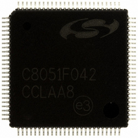
C8051F042-GQ Silicon Laboratories Inc, C8051F042-GQ Datasheet - Page 219

C8051F042-GQ
Manufacturer Part Number
C8051F042-GQ
Description
IC 8051 MCU 64K FLASH 100TQFP
Manufacturer
Silicon Laboratories Inc
Series
C8051F04xr
Datasheets
1.C8051F040-TB.pdf
(328 pages)
2.C8051F042-GQ.pdf
(2 pages)
3.C8051F042-GQ.pdf
(16 pages)
Specifications of C8051F042-GQ
Program Memory Type
FLASH
Program Memory Size
64KB (64K x 8)
Package / Case
100-TQFP, 100-VQFP
Core Processor
8051
Core Size
8-Bit
Speed
25MHz
Connectivity
CAN, EBI/EMI, SMBus (2-Wire/I²C), SPI, UART/USART
Peripherals
Brown-out Detect/Reset, POR, PWM, Temp Sensor, WDT
Number Of I /o
64
Ram Size
4.25K x 8
Voltage - Supply (vcc/vdd)
2.7 V ~ 3.6 V
Data Converters
A/D 8x8b, 13x10b; D/A 2x10b, 2x12b
Oscillator Type
Internal
Operating Temperature
-40°C ~ 85°C
Processor Series
C8051F0x
Core
8051
Data Bus Width
8 bit
Data Ram Size
4.25 KB
Interface Type
CAN/SMBus/SPI/UART
Maximum Clock Frequency
25 MHz
Number Of Programmable I/os
64
Number Of Timers
5
Operating Supply Voltage
2.7 V to 3.6 V
Maximum Operating Temperature
+ 85 C
Mounting Style
SMD/SMT
3rd Party Development Tools
PK51, CA51, A51, ULINK2
Development Tools By Supplier
C8051F040DK
Minimum Operating Temperature
- 40 C
On-chip Adc
8-ch x 8-bit or 13-ch x 12-bit
On-chip Dac
2-ch x 12-bit
Lead Free Status / RoHS Status
Lead free / RoHS Compliant
For Use With
336-1205 - DEV KIT FOR F040/F041/F042/F043
Eeprom Size
-
Lead Free Status / Rohs Status
Lead free / RoHS Compliant
Other names
336-1207
Available stocks
Company
Part Number
Manufacturer
Quantity
Price
Company:
Part Number:
C8051F042-GQ
Manufacturer:
Silicon Laboratories Inc
Quantity:
10 000
Company:
Part Number:
C8051F042-GQR
Manufacturer:
Silicon Laboratories Inc
Quantity:
10 000
- Current page: 219 of 328
- Download datasheet (3Mb)
Bits7-0:
Note:
Bits7-0:
Note:
P3.7
R/W
R/W
Bit7
Bit7
P2MDOUT.[7:0]: Port2 Output Mode Bits.
0: Port Pin output mode is configured as Open-Drain.
1: Port Pin output mode is configured as Push-Pull.
SDA, SCL, and RX0 (when UART0 is in Mode 0) and RX1 (when UART1 is in Mode 0) are
always configured as Open-Drain when they appear on Port pins.
P3.[7:0]: Port3 Output Latch Bits.
(Write - Output appears on I/O pins per XBR0, XBR1, XBR2, and XBR3 Registers)
0: Logic Low Output.
1: Logic High Output (open if corresponding P3MDOUT.n bit = 0).
(Read - Regardless of XBR0, XBR1, XBR2, and XBR3 Register settings).
0: P3.n pin is logic low.
1: P3.n pin is logic high.
P3.[7:0] can be driven by the External Data Memory Interface (as AD[7:0] in Multiplexed
mode, or as D[7:0] in Non-multiplexed mode). See
Interface and On-Chip XRAM” on page 187
ory Interface.
P3.6
R/W
R/W
Bit6
Bit6
SFR Definition 17.12. P2MDOUT: Port2 Output Mode
P3.5
R/W
R/W
Bit5
Bit5
SFR Definition 17.13. P3: Port3 Data
P3.4
R/W
R/W
Bit4
Bit4
Rev. 1.5
P3.3
R/W
R/W
Bit3
Bit3
C8051F040/1/2/3/4/5/6/7
for more information about the External Mem-
P3.2
R/W
R/W
Bit2
Bit2
Section “16. External Data Memory
P3.1
R/W
R/W
Bit1
Bit1
SFR Address:
SFR Address:
SFR Page:
SFR Page:
P3.0
R/W
Bit0
R/W
Bit0
0xA6
F
00000000
0xB0
All Pages
Reset Value
Addressable
Reset Value
11111111
Bit
219
Related parts for C8051F042-GQ
Image
Part Number
Description
Manufacturer
Datasheet
Request
R
Part Number:
Description:
SMD/C°/SINGLE-ENDED OUTPUT SILICON OSCILLATOR
Manufacturer:
Silicon Laboratories Inc
Part Number:
Description:
Manufacturer:
Silicon Laboratories Inc
Datasheet:
Part Number:
Description:
N/A N/A/SI4010 AES KEYFOB DEMO WITH LCD RX
Manufacturer:
Silicon Laboratories Inc
Datasheet:
Part Number:
Description:
N/A N/A/SI4010 SIMPLIFIED KEY FOB DEMO WITH LED RX
Manufacturer:
Silicon Laboratories Inc
Datasheet:
Part Number:
Description:
N/A/-40 TO 85 OC/EZLINK MODULE; F930/4432 HIGH BAND (REV E/B1)
Manufacturer:
Silicon Laboratories Inc
Part Number:
Description:
EZLink Module; F930/4432 Low Band (rev e/B1)
Manufacturer:
Silicon Laboratories Inc
Part Number:
Description:
I°/4460 10 DBM RADIO TEST CARD 434 MHZ
Manufacturer:
Silicon Laboratories Inc
Part Number:
Description:
I°/4461 14 DBM RADIO TEST CARD 868 MHZ
Manufacturer:
Silicon Laboratories Inc
Part Number:
Description:
I°/4463 20 DBM RFSWITCH RADIO TEST CARD 460 MHZ
Manufacturer:
Silicon Laboratories Inc
Part Number:
Description:
I°/4463 20 DBM RADIO TEST CARD 868 MHZ
Manufacturer:
Silicon Laboratories Inc
Part Number:
Description:
I°/4463 27 DBM RADIO TEST CARD 868 MHZ
Manufacturer:
Silicon Laboratories Inc
Part Number:
Description:
I°/4463 SKYWORKS 30 DBM RADIO TEST CARD 915 MHZ
Manufacturer:
Silicon Laboratories Inc
Part Number:
Description:
N/A N/A/-40 TO 85 OC/4463 RFMD 30 DBM RADIO TEST CARD 915 MHZ
Manufacturer:
Silicon Laboratories Inc
Part Number:
Description:
I°/4463 20 DBM RADIO TEST CARD 169 MHZ
Manufacturer:
Silicon Laboratories Inc


