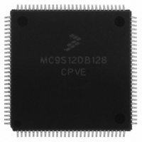
MC9S12DB128CPVE Freescale Semiconductor, MC9S12DB128CPVE Datasheet - Page 72

MC9S12DB128CPVE
Manufacturer Part Number
MC9S12DB128CPVE
Description
IC MCU 128K FLASH 25MHZ 112-LQFP
Manufacturer
Freescale Semiconductor
Series
HCS12r
Datasheets
1.MC9S12DG128CFUER.pdf
(128 pages)
2.MC9S12DB128CPVE.pdf
(142 pages)
3.MC9S12DB128CPVE.pdf
(12 pages)
Specifications of MC9S12DB128CPVE
Core Processor
HCS12
Core Size
16-Bit
Speed
25MHz
Connectivity
CAN, I²C, SCI, SPI
Peripherals
PWM, WDT
Number Of I /o
91
Program Memory Size
128KB (128K x 8)
Program Memory Type
FLASH
Eeprom Size
2K x 8
Ram Size
8K x 8
Voltage - Supply (vcc/vdd)
2.35 V ~ 5.25 V
Data Converters
A/D 16x10b
Oscillator Type
Internal
Operating Temperature
-40°C ~ 85°C
Package / Case
112-LQFP
Controller Family/series
HCS12/S12X
No. Of I/o's
91
Eeprom Memory Size
2048Byte
Ram Memory Size
8192Byte
Cpu Speed
25MHz
Rohs Compliant
Yes
Package
112LQFP
Family Name
HCS12
Maximum Speed
50 MHz
Operating Supply Voltage
3.3|5 V
Data Bus Width
16 Bit
Number Of Programmable I/os
91
Interface Type
CAN/SCI/SPI
On-chip Adc
2(8-chx10-bit)
Number Of Timers
8
Lead Free Status / RoHS Status
Lead free / RoHS Compliant
Available stocks
Company
Part Number
Manufacturer
Quantity
Price
Company:
Part Number:
MC9S12DB128CPVE
Manufacturer:
Freescale Semiconductor
Quantity:
10 000
Company:
Part Number:
MC9S12DB128CPVER
Manufacturer:
Freescale Semiconductor
Quantity:
10 000
Device User Guide — 9S12DT128DGV2/D V02.15
2.3.51 PS5 / MOSI0 — Port S I/O Pin 5
PS5 is a general purpose input or output pin. It can be configured as master output (during master mode)
or slave input pin (during slave mode) MOSI of the Serial Peripheral Interface 0 (SPI0).
2.3.52 PS4 / MISO0 — Port S I/O Pin 4
PS4 is a general purpose input or output pin. It can be configured as master input (during master mode) or
slave output pin (during slave mode) MOSI of the Serial Peripheral Interface 0 (SPI0).
2.3.53 PS3 / TXD1 — Port S I/O Pin 3
PS3 is a general purpose input or output pin. It can be configured as the transmit pin TXD of Serial
Communication Interface 1 (SCI1).
2.3.54 PS2 / RXD1 — Port S I/O Pin 2
PS2 is a general purpose input or output pin. It can be configured as the receive pin RXD of Serial
Communication Interface 1 (SCI1).
2.3.55 PS1 / TXD0 — Port S I/O Pin 1
PS1 is a general purpose input or output pin. It can be configured as the transmit pin TXD of Serial
Communication Interface 0 (SCI0).
2.3.56 PS0 / RXD0 — Port S I/O Pin 0
PS0 is a general purpose input or output pin. It can be configured as the receive pin RXD of Serial
Communication Interface 0 (SCI0).
2.3.57 PT[7:0] / IOC[7:0] — Port T I/O Pins [7:0]
PT7-PT0 are general purpose input or output pins. They can be configured as input capture or output
compare pins IOC7-IOC0 of the Enhanced Capture Timer (ECT).
2.4 Power Supply Pins
MC9S12DT128 power and ground pins are described below.
72
Mnemonic
VDD1, 2
VSS1, 2
Table 2-2 MC9S12DT128 Power and Ground Connection Summary
112-pin QFP
Pin Number
13, 65
14, 66
Nominal
Voltage
2.5V
0V
Internal power and ground generated by internal regulator
Description
Freescale Semiconductor


