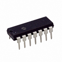
PIC16HV610-I/P Microchip Technology, PIC16HV610-I/P Datasheet - Page 25

PIC16HV610-I/P
Manufacturer Part Number
PIC16HV610-I/P
Description
IC PIC MCU FLASH 1KX14 14DIP
Manufacturer
Microchip Technology
Series
PIC® 16Fr
Datasheets
1.PIC12F609T-ISN.pdf
(26 pages)
2.PIC16F616T-ISL.pdf
(214 pages)
3.PIC16F616T-ISL.pdf
(8 pages)
4.PIC16HV616-ISL.pdf
(26 pages)
Specifications of PIC16HV610-I/P
Core Size
8-Bit
Program Memory Size
1.75KB (1K x 14)
Peripherals
Brown-out Detect/Reset, POR, WDT
Core Processor
PIC
Speed
20MHz
Number Of I /o
11
Program Memory Type
FLASH
Ram Size
64 x 8
Voltage - Supply (vcc/vdd)
2 V ~ 5 V
Oscillator Type
Internal
Operating Temperature
-40°C ~ 85°C
Package / Case
14-DIP (0.300", 7.62mm)
Controller Family/series
PIC16HV
No. Of I/o's
12
Ram Memory Size
64Byte
Cpu Speed
20MHz
Processor Series
PIC16H
Core
PIC
Data Bus Width
8 bit
Data Ram Size
64 B
Interface Type
RS-232 , USB
Maximum Clock Frequency
20 MHz
Number Of Programmable I/os
11
Number Of Timers
2
Maximum Operating Temperature
+ 85 C
Mounting Style
Through Hole
3rd Party Development Tools
52715-96, 52716-328, 52717-734
Development Tools By Supplier
PG164130, DV164035, DV244005, DV164005, PG164120, ICE2000
Minimum Operating Temperature
- 40 C
Lead Free Status / RoHS Status
Lead free / RoHS Compliant
For Use With
AC162083 - HEADER MPLAB ICD2 PIC16F616 8/14ICE2000 - EMULATOR MPLAB-ICE 2000 PODAC124001 - MODULE SKT PROMATEII 8DIP/SOIC
Eeprom Size
-
Data Converters
-
Connectivity
-
Lead Free Status / Rohs Status
Details
Available stocks
Company
Part Number
Manufacturer
Quantity
Price
Company:
Part Number:
PIC16HV610-I/P
Manufacturer:
Microchip
Quantity:
1 670
- PIC12F609T-ISN PDF datasheet
- PIC16F616T-ISL PDF datasheet #2
- PIC16F616T-ISL PDF datasheet #3
- PIC16HV616-ISL PDF datasheet #4
- Current page: 25 of 214
- Download datasheet (4Mb)
FIGURE 2-6:
FIGURE 2-7:
© 2009 Microchip Technology Inc.
Bank Select
Bank Select
RP1
RP1
For memory map detail, see Figure 2-3.
Note 1: The RP1 and IRP bits are reserved; always maintain these bits clear.
For memory map detail, see Figure 2-4.
Note 1: The RP1 and IRP bits are reserved; always maintain these bits clear.
(1)
(1)
Unimplemented data memory locations, read as ‘0’.
Unimplemented data memory locations, read as ‘0’.
RP0
RP0
2: Accesses in Bank 2 and Bank 3 are mirrored back into Bank 0 and Bank 1, respectively.
2: Accesses in Bank 2 and Bank 3 are mirrored back into Bank 0 and Bank 1, respectively.
Direct Addressing
Direct Addressing
6
6
Data
Memory
Data
Memory
Location Select
Location Select
DIRECT/INDIRECT ADDRESSING PIC16F610/16HV610
DIRECT/INDIRECT ADDRESSING PIC16F616/16HV616
From Opcode
From Opcode
7Fh
7Fh
00h
00h
Bank 0
Bank 0
00
00
0
0
PIC16F610/616/16HV610/616
Bank 1
Bank 1
01
01
Bank 2
Bank 2
10
10
NOT USED
NOT USED
Bank 3
Bank 3
11
11
(2)
(2)
IRP
IRP
Bank Select
Bank Select
180h
180h
(1)
(1)
1FFh
1FFh
7
7
Indirect Addressing
Indirect Addressing
File Select Register
File Select Register
DS41288F-page 25
Location Select
Location Select
0
0
Related parts for PIC16HV610-I/P
Image
Part Number
Description
Manufacturer
Datasheet
Request
R

Part Number:
Description:
Manufacturer:
Microchip Technology Inc.
Datasheet:

Part Number:
Description:
Manufacturer:
Microchip Technology Inc.
Datasheet:

Part Number:
Description:
Manufacturer:
Microchip Technology Inc.
Datasheet:

Part Number:
Description:
Manufacturer:
Microchip Technology Inc.
Datasheet:

Part Number:
Description:
Manufacturer:
Microchip Technology Inc.
Datasheet:

Part Number:
Description:
Manufacturer:
Microchip Technology Inc.
Datasheet:

Part Number:
Description:
Manufacturer:
Microchip Technology Inc.
Datasheet:

Part Number:
Description:
Manufacturer:
Microchip Technology Inc.
Datasheet:


