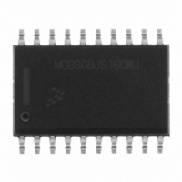
MC9S08JS16CWJ Freescale Semiconductor, MC9S08JS16CWJ Datasheet - Page 7

MC9S08JS16CWJ
Manufacturer Part Number
MC9S08JS16CWJ
Description
IC MCU 8BIT 16K FLASH 20SOIC
Manufacturer
Freescale Semiconductor
Series
HCS08r
Datasheet
1.DEMO9S08JS16.pdf
(32 pages)
Specifications of MC9S08JS16CWJ
Core Processor
HCS08
Core Size
8-Bit
Speed
48MHz
Connectivity
LIN, SCI, SPI, USB
Peripherals
LVD, POR, PWM
Number Of I /o
14
Program Memory Size
16KB (16K x 8)
Program Memory Type
FLASH
Ram Size
512 x 8
Voltage - Supply (vcc/vdd)
2.7 V ~ 5.5 V
Oscillator Type
Internal
Operating Temperature
-40°C ~ 85°C
Package / Case
20-SOIC (7.5mm Width)
Processor Series
S08JS
Core
HCS08
Data Bus Width
8 bit
Data Ram Size
256 B
Interface Type
SCI, SPI
Maximum Clock Frequency
48 MHz
Number Of Programmable I/os
14
Number Of Timers
1
Operating Supply Voltage
2.7 V to 5.5 V
Maximum Operating Temperature
+ 85 C
Mounting Style
SMD/SMT
3rd Party Development Tools
EWS08
Development Tools By Supplier
DEMO9S08JS16
Minimum Operating Temperature
- 40 C
Controller Family/series
HCS08
No. Of I/o's
14
Ram Memory Size
512Byte
Cpu Speed
8MHz
No. Of Timers
1
Embedded Interface Type
SCI, SPI, USB
Rohs Compliant
Yes
Cpu Family
HCS08
Device Core Size
8b
Frequency (max)
48MHz
Total Internal Ram Size
512KB
Number Of Timers - General Purpose
1
Operating Supply Voltage (typ)
3.3/5V
Operating Supply Voltage (max)
5.5V
Operating Supply Voltage (min)
2.7V
Instruction Set Architecture
CISC
Operating Temp Range
-40C to 85C
Operating Temperature Classification
Industrial
Mounting
Surface Mount
Pin Count
20
Package Type
SOIC W
For Use With
DEMO9S08JS16 - BOARD DEMO FOR JS16 FAMILY
Lead Free Status / RoHS Status
Lead free / RoHS Compliant
Eeprom Size
-
Data Converters
-
Lead Free Status / Rohs Status
Lead free / RoHS Compliant
Available stocks
Company
Part Number
Manufacturer
Quantity
Price
Company:
Part Number:
MC9S08JS16CWJ
Manufacturer:
Renesas
Quantity:
119
Part Number:
MC9S08JS16CWJ
Manufacturer:
FREESCALE
Quantity:
20 000
3.3
This section provides information about operating temperature range, power dissipation, and package
thermal resistance. Power dissipation on I/O pins is usually small compared to the power dissipation in
on-chip logic and it is user-determined rather than being controlled by the MCU design. In order to take
P
V
loads), the difference between pin voltage and V
The average chip-junction temperature (T
where:
T
θ
Freescale Semiconductor
JA
I/O
A
DD
= Ambient temperature, °C
= Package thermal resistance, junction-to-ambient, °C/W
into account in power calculations, determine the difference between actual pin voltage and V
and multiply by the pin current for each I/O pin. Except in cases of unusually high pin current (heavy
Thermal Characteristics
1
2
3
1
2
3
4
Operating temperature range (packaged)
Thermal resistance
24-pin QFN
20-pin SOIC
Input must be current limited to the value specified. To determine the value of the required
current-limiting resistor, calculate resistance values for positive (V
voltages, then use the larger of the two resistance values.
All functional non-supply pins are internally clamped to V
Power supply must maintain regulation within operating V
operating maximum current conditions. If positive injection current (V
I
out of regulation. Ensure external V
current. This will be the greatest risk when the MCU is not consuming power. Examples are: if
no system clock is present, or if the clock rate is very low which would reduce overall power
consumption.
Junction temperature is a function of die size, on-chip power dissipation, package thermal
resistance, mounting site (board) temperature, ambient temperature, air flow, power dissipation
of other components on the board, and board thermal resistance
Junction to Ambient Natural Convection
1s — Single layer board, one signal layer
2s2p — Four layer board, 2 signal and 2 power layers
DD
, the injection current may flow out of V
1,2,3,4
MC9S08JS16 Series MCU Data Sheet, Rev. 4
Rating
Table 4. Thermal Characteristics
T
J
J
) in °C can be obtained from:
= T
DD
A
load will shunt current greater than maximum injection
+ (P
SS
DD
or V
D
and could result in external power supply going
× θ
2s2p
2s2p
DD
JA
1s
1s
)
will be very small.
SS
DD
Symbol
and V
range during instantaneous and
θ
T
JA
A
DD
DD
) and negative (V
.
In
> V
-40 to 85
T
Value
L
DD
92
33
86
58
to T
) is greater than
H
Electrical Characteristics
SS
) clamp
°C/W
Unit
°C
SS
Eqn. 1
or
7


