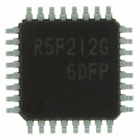
R5F212G6SDFP#U0 Renesas Electronics America, R5F212G6SDFP#U0 Datasheet - Page 9

R5F212G6SDFP#U0
Manufacturer Part Number
R5F212G6SDFP#U0
Description
IC R8C/2G MCU FLASH 32K 32-LQFP
Manufacturer
Renesas Electronics America
Series
R8C/2x/2Gr
Datasheet
1.R5F212G4SDFPU0.pdf
(45 pages)
Specifications of R5F212G6SDFP#U0
Core Processor
R8C
Core Size
16/32-Bit
Speed
8MHz
Connectivity
LIN, SIO, UART/USART
Peripherals
POR, PWM, Voltage Detect, WDT
Number Of I /o
27
Program Memory Size
32KB (32K x 8)
Program Memory Type
FLASH
Ram Size
1K x 8
Voltage - Supply (vcc/vdd)
2.2 V ~ 5.5 V
Oscillator Type
Internal
Operating Temperature
-40°C ~ 85°C
Package / Case
32-LQFP
Lead Free Status / RoHS Status
Lead free / RoHS Compliant
Eeprom Size
-
Data Converters
-
Available stocks
Company
Part Number
Manufacturer
Quantity
Price
R8C/2G Group
Rev.1.00
REJ03B0223-0100
1.5
Table 1.4
I: Input
NOTE:
Power supply input VCC, VSS
Reset input
MODE
XCIN clock input
XCIN clock output
INT interrupt input
Key input interrupt
Timer RA
Timer RB
Timer RE
Timer RF
Serial interface
Comparator
I/O port
Output port
Table 1.4 lists Pin Functions.
1. Refer to the oscillator manufacturer for oscillation characteristics.
Type
Pin Functions
Apr 04, 2008
O: Output
Pin Functions
RESET
MODE
XCIN
XCOUT
INT0 to INT2, INT4
KI0 to KI3
TRAIO
TRAO
TRBO
TREO
TRFI
TRFO00 to TRFO02,
TRFO10 to TRFO12
CLK0, CLK2
RXD0, RXD2
TXD0, TXD2
VCMP1, VCMP2
CVREF
VCOUT1, VCOUT2
P0_4 to P0_7,
P1_0 to P1_7,
P3_0 to P3_7,
P4_3, P4_5,
P6_0, P6_3 to P6_6
P4_4
Page 7 of 41
Symbol
I/O: Input and output
I/O Type
I/O
I/O
I/O
O
O
O
O
O
O
O
O
–
I
I
I
I
I
I
I
I
I
Apply 2.2 V to 5.5 V to the VCC pin. Apply 0 V to the VSS pin.
Input “L” on this pin resets the MCU.
Connect this pin to VCC via a resistor.
These pins are provided for XCIN clock generation circuit I/O.
Connect a crystal oscillator between the XCIN and XCOUT
pins.
leave the XCOUT pin open.
INT interrupt input pins
Key input interrupt input pins
Timer RA I/O pin
Timer RA output pin
Timer RB output pin
Divided clock output pin
Timer RF input pin
Timer RF output pins
Clock I/O pin
Serial data input pin
Serial data output pin
Analog input pins to comparator
Reference voltage input pin to comparator
Comparator output pins
CMOS I/O ports. Each port has an I/O select direction
register, allowing each pin in the port to be directed for input
or output individually.
Any port set to input can be set to use a pull-up resistor or not
by a program.
Output-only port
(1)
To use an external clock, input it to the XCIN pin and
Description
1. Overview


