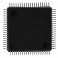
M38869FFAGP#U0 Renesas Electronics America, M38869FFAGP#U0 Datasheet - Page 82

M38869FFAGP#U0
Manufacturer Part Number
M38869FFAGP#U0
Description
IC 740/3886 MCU FLASH 80QFP
Manufacturer
Renesas Electronics America
Series
740/38000r
Datasheet
1.M38869FFAGPU0.pdf
(113 pages)
Specifications of M38869FFAGP#U0
Core Processor
740
Core Size
8-Bit
Speed
10MHz
Connectivity
I²C, SIO, UART/USART
Peripherals
PWM, WDT
Number Of I /o
64
Program Memory Size
60KB (60K x 8)
Program Memory Type
FLASH
Ram Size
2K x 8
Voltage - Supply (vcc/vdd)
4 V ~ 5.5 V
Data Converters
A/D 8x10b; D/A 2x8b
Oscillator Type
Internal
Operating Temperature
-20°C ~ 85°C
Package / Case
80-QFP
Lead Free Status / RoHS Status
Lead free / RoHS Compliant
Eeprom Size
-
Available stocks
Company
Part Number
Manufacturer
Quantity
Price
Input command code 80
M38869FFAHP/GP outputs error information from the SDA pin,
beginning at the next falling edge of the serial clock. If the LSB bit
of the 8-bit error information is 1, it indicates that a command error
has occurred. A command error means that some invalid com-
mands other than commands shown in Table 26 has been input.
When a command error occurs, the serial communication circuit
sets the corresponding flag and stops functioning to avoid an erro-
neous programming or erase. When being placed in this state, the
serial communication circuit does not accept the subsequent serial
clock and data (even including an error check command). There-
fore, if the user wants to execute an error check command,
Fig. 78 Timings at error checking
Note: The programming/erasing algorithm flow chart of the serial
Error check command
I/O mode is the same as that of the parallel I/O mode. Re-
fer to Figure 71.
Note: When outputting the error flag, the SDA pin is switched for output at the first falling edge of the serial clock. The SDA pin is placed
in the floating state during the period of th
16
SCLK
SDA
OE
BUSY
in the first transfer, and the
“L”
“H”
Command code input (80
0 0 0 0 0 0 0 1
(C-E)
after the last rising edge of the serial clock (at the 8th bit).
16
)
t
CH
temporarily drop the V
the serial input/output mode. Then, place the M38869FFAHP/GP
into the serial I/O mode back again. The serial communication cir-
cuit is reset by this operation and is ready to accept commands.
The error flag alone is not cleared by this operation, so the user
can examine the serial communication circuit’s error conditions
before reset. This examination is done by the first execution of an
error check command after the reset. The error flag is cleared
when the user has executed the error check command. Because
the error flag is undefined immediately after power-on, always be
sure to execute the error check command.
E0
Error flag output
?
? ? ? ? ? ?
SINGLE-CHIP 8-BIT CMOS MICROCOMPUTER
MITSUBISHI MICROCOMPUTERS
PP
pin input to the V
3886 Group
PP
L level to terminate
79


