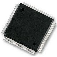
MCF53013CQT240 Freescale Semiconductor, MCF53013CQT240 Datasheet - Page 22

MCF53013CQT240
Manufacturer Part Number
MCF53013CQT240
Description
MCU 32BIT COLDFIRE EMAC 208LQFP
Manufacturer
Freescale Semiconductor
Series
MCF5301xr
Datasheet
1.MCF53010CQT240.pdf
(62 pages)
Specifications of MCF53013CQT240
Core Processor
Coldfire V3
Core Size
32-Bit
Speed
240MHz
Connectivity
EBI/EMI, Ethernet, I²C, MMC, SPI, SSI, UART/USART, USB OTG
Peripherals
DMA, PWM, WDT
Number Of I /o
61
Program Memory Size
16KB (16K x 8)
Program Memory Type
Cache
Ram Size
128K x 8
Voltage - Supply (vcc/vdd)
1.08 V ~ 3.6 V
Oscillator Type
Internal
Operating Temperature
-40°C ~ 85°C
Package / Case
208-LQFP
Processor Series
MCF5301x
Core
ColdFire V3
Data Bus Width
32 bit
Data Ram Size
128 KB
Interface Type
UART, I2C, SPI, SSI, Ethernet
Maximum Clock Frequency
20 MHz to 400 MHz
Number Of Programmable I/os
61
Number Of Timers
8
Operating Supply Voltage
3.6 V
Maximum Operating Temperature
+ 85 C
Mounting Style
SMD/SMT
3rd Party Development Tools
JLINK-CF-BDM26, EWCF
Development Tools By Supplier
M53015EVB, M53017KIT, M53017MOD
Minimum Operating Temperature
- 40 C
Lead Free Status / RoHS Status
Lead free / RoHS Compliant
Eeprom Size
-
Data Converters
-
Preliminary Electrical Characteristics
5.4.1
To further enhance noise isolation, an external filter is strongly recommended for PLL analog V
Figure 8
close to the dedicated PLLV
5.4.2
To minimize noise, external filters are required for each of the USB power pins. The filter shown in
connected between the board EV
close to the dedicated USBV
22
1
2
3
SDRAM and FlexBus Output High Voltage
SDRAM and FlexBus Output Low Voltage
Input Leakage Current
Weak Internal Pull-Up/Pull-down Device Current
Selectable Weak Internal Pull-Up/Pull-down Device Current
Input Capacitance
Mobile DDR/Bus Input High Voltage (nominal 1.8V)
DDR/Bus Pad Supply Voltage (nominal 2.5V)
SDR/Bus Pad Supply Voltage (nominal 3.3V)
I
Mobile DDR/Bus Input High Voltage (nominal 1.8V)
DDR/Bus Pad Supply Voltage (nominal 2.5V)
SDR/Bus Pad Supply Voltage (nominal 3.3V)
I
V
All input-only pins
All input/output (three-state) pins
Refer to the signals section for pins having weak internal pull-up devices.
Refer to the signals section for pins having weak internal pull-up devices.
This parameter is characterized before qualification rather than 100% tested.
OH
OL
in
= 5.0 mA for all modes
= V
= –5.0 mA for all modes
should be connected between the board V
DD
PLL Power Filtering
USB Power Filtering
or V
SS
, Input-only pins
3
Board IV
DD
DD
Characteristic
pin as possible.
pin as possible.
DD
Table 10. DC Electrical Specifications (continued)
DD
or IV
Preliminary—Subject to Change Without Notice
Figure 8. System PLL V
DD
10 Ω
and each of the USBV
MCF5301x Data Sheet, Rev. 5
1
DD
and the PLLV
10 µF
GND
2
DD
DD
DD
pins. The resistor and capacitors should be placed as
Power Filter
pins. The resistor and capacitors should be placed as
0.1 µF
Symbol
SDV
SDV
I
I
APU
APU
C
I
in
in
OH
OL
SDV
SDVDD × 0.9
PLL V
DD
–2.5
Min
2.9
10
25
—
—
—
—
—
DD
– 0.35
DD
Pin
pins. The filter shown in
Figure 2
Freescale Semiconductor
SDV
Max
0.35
DD
315
150
0.4
2.5
—
—
—
7
7
should be
× 0.1
Unit
μA
μA
μA
pF
V
V


