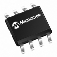
PIC12F510-E/MS Microchip Technology, PIC12F510-E/MS Datasheet - Page 17

PIC12F510-E/MS
Manufacturer Part Number
PIC12F510-E/MS
Description
IC PIC MCU FLASH 1KX14 8MSOP
Manufacturer
Microchip Technology
Series
PIC® 12Fr
Datasheets
1.PIC12F510-ISN.pdf
(124 pages)
2.PIC12F510-ISN.pdf
(8 pages)
3.PIC12F510-ISN.pdf
(20 pages)
Specifications of PIC12F510-E/MS
Core Processor
PIC
Core Size
8-Bit
Speed
8MHz
Peripherals
POR, WDT
Number Of I /o
5
Program Memory Size
1.5KB (1K x 12)
Program Memory Type
FLASH
Ram Size
38 x 8
Voltage - Supply (vcc/vdd)
2 V ~ 5.5 V
Data Converters
A/D 4x8b
Oscillator Type
Internal
Operating Temperature
-40°C ~ 125°C
Package / Case
8-MSOP, Micro8™, 8-uMAX, 8-uSOP,
Processor Series
PIC12F
Core
PIC
Data Bus Width
8 bit
Data Ram Size
38 B
Maximum Clock Frequency
8 MHz
Number Of Programmable I/os
5
Number Of Timers
1
Maximum Operating Temperature
+ 125 C
Mounting Style
SMD/SMT
3rd Party Development Tools
52715-96, 52716-328, 52717-734
Development Tools By Supplier
PG164130, DV164035, DV244005, DV164005, PG164120, DV164101, DV164120, DM163029
Minimum Operating Temperature
- 40 C
On-chip Adc
8 bit, 3 Channel
For Use With
AC162070 - HEADER INTRFC MPLAB ICD2 8/14PAC164325 - MODULE SKT FOR 8MSOP
Lead Free Status / RoHS Status
Lead free / RoHS Compliant
Eeprom Size
-
Connectivity
-
Lead Free Status / Rohs Status
Details
6.0
TABLE 6-1:
© 2007 Microchip Technology Inc.
AC/DC CHARACTERISTICS
General
V
V
I
I
V
I
T
T
V
V
T
T
Serial Program/Verify
T
T
T
T
T
T
T
T
T
Note 1:
DDPROG
DDERA
PP
SET
SET
ERA
RESET
VHHR
PPDP
IH
IL
HLD
HLD
DLY
DLY
DLY
PROG
DIS
DDPROG
DDERA
PP
Sym.
1
1
0
1
0
1
1
2
3
PROGRAM/VERIFY MODE ELECTRICAL CHARACTERISTICS
V
program memory
V
memory
I
program memory
I
memory
High voltage on MCLR for Program/Verify
mode entry
MCLR pin current during Program/Verify
mode
MCLR rise time (V
Verify mode entry
Hold time after V
(ICSPCLK, ICSPDAT) input high-level
(ICSPCLK, ICSPDAT) input low-level
ICSPCLK, ICSPDAT setup time before
MCLR↑ (Program/Verify mode selection
pattern setup time)
ICSPCLK, ICSPDAT hold time after MCLR↑
(Program/Verify mode selection pattern setup
time)
Data in setup time before clock↓
Data in hold time after clock↓
Data input not driven to next clock input (delay
required between command/data or
command/command)
Delay between clock↓ to clock↑ of next
command or data
Clock↑ to data out valid (during Read Data)
Erase cycle time
Programming cycle time (externally timed)
Time delay for internal programming voltage
discharge
Time between exiting Program mode with V
and V
mode by applying V
Minimum time to ensure that function completes successfully over voltage, temperature and device variations.
DD
DD
DD
DD
level for programming operations,
level for Bulk Erase operations, program
level for programming operations,
level for Bulk Erase operations, program
PP
AC/DC CHARACTERISTICS TIMING REQUIREMENTS FOR PROGRAM/VERIFY
MODE
at G
ND
Characteristics
and then re-entering Program
PP
SS
↑
DD
to V
.
IHH
) for Program/
DD
Standard Operating Conditions (unless otherwise stated)
Operating Temperature
Operating Voltage
0.8 V
Min.
12.5
100
100
100
100
4.5
4.5
1.0
1.0
—
—
—
—
—
—
—
—
—
5
5
DD
Typ.
10
—
—
—
—
—
—
—
—
—
—
—
—
—
—
—
—
—
—
—
—
0.2 V
Max.
10
13.5
0.45
2
5.5
5.5
0.5
0.5
1.0
80
—
—
—
—
—
—
—
—
—
—
(1)
(1)
10°C ≤ T
4.5V ≤ V
DD
Units
mA
mA
mA
ms
ms
ms
A
DD
PIC12F510
μs
μs
ns
μs
ns
ns
μs
μs
ns
μs
V
V
V
V
V
≤ 40°C
≤ 5.5V
DS41257B-page 17
Conditions/
Comments


