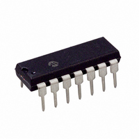
PIC16F684-E/P Microchip Technology, PIC16F684-E/P Datasheet - Page 71

PIC16F684-E/P
Manufacturer Part Number
PIC16F684-E/P
Description
IC PIC MCU FLASH 2KX14 14DIP
Manufacturer
Microchip Technology
Series
PIC® 16Fr
Datasheets
1.PIC16F616T-ISL.pdf
(8 pages)
2.PIC16F688T-ISL.pdf
(688 pages)
3.PIC16F684-ISL.pdf
(4 pages)
4.PIC16F684-ISL.pdf
(192 pages)
5.PIC16F684-ISL.pdf
(6 pages)
6.PIC16F684-IST.pdf
(164 pages)
Specifications of PIC16F684-E/P
Program Memory Type
FLASH
Program Memory Size
3.5KB (2K x 14)
Package / Case
14-DIP (0.300", 7.62mm)
Core Processor
PIC
Core Size
8-Bit
Speed
20MHz
Peripherals
Brown-out Detect/Reset, POR, PWM, WDT
Number Of I /o
12
Eeprom Size
256 x 8
Ram Size
128 x 8
Voltage - Supply (vcc/vdd)
2 V ~ 5.5 V
Data Converters
A/D 8x10b
Oscillator Type
Internal
Operating Temperature
-40°C ~ 125°C
Processor Series
PIC16F
Core
PIC
Data Bus Width
8 bit
Data Ram Size
128 B
Maximum Clock Frequency
20 MHz
Number Of Programmable I/os
12
Number Of Timers
3
Operating Supply Voltage
2 V to 5.5 V
Maximum Operating Temperature
+ 125 C
Mounting Style
Through Hole
3rd Party Development Tools
52715-96, 52716-328, 52717-734
Development Tools By Supplier
PG164130, DV164035, DV244005, DV164005, PG164120, ICE2000, DM163014, DM164120-4
Minimum Operating Temperature
- 40 C
On-chip Adc
8-ch x 10-bit
Lead Free Status / RoHS Status
Lead free / RoHS Compliant
For Use With
DM163029 - BOARD PICDEM FOR MECHATRONICSACICE0207 - MPLABICE 14P 300 MIL ADAPTER
Connectivity
-
Lead Free Status / Rohs Status
Lead free / RoHS Compliant
9.3
The A/D converter module can operate during Sleep.
This requires the A/D clock source to be set to the
internal oscillator. When the RC clock source is
selected, the A/D waits one instruction before starting
the conversion. This allows the SLEEP instruction to be
executed, thus eliminating much of the switching noise
from the conversion. When the conversion is complete,
the GO/DONE bit is cleared and the result is loaded
into the ADRESH:ADRESL registers.
FIGURE 9-5:
9.4
A device Reset forces all registers to their Reset state.
Thus, the A/D module is turned off and any pending
conversion
registers are unchanged.
9.5
An A/D conversion can be started by the “special event
trigger” of the ECCP module. This requires that the
CCP1M3:CCP1M0
programmed as ‘1011’ and that the A/D module is
enabled (ADON bit is set). When the trigger occurs, the
GO/DONE bit will be set, starting the A/D conversion
and the Timer1 counter will be reset to zero. Timer1 is
reset to automatically repeat the A/D acquisition period
with
ADRESH:ADRESL to the desired location).
2004 Microchip Technology Inc.
minimal
A/D Operation During Sleep
Effects of Reset
Use of the ECCP Trigger
is
software
aborted.
A/D TRANSFER FUNCTION
bits
0V
3FDh
3FCh
3FEh
3FBh
3FFh
004h
003h
002h
001h
000h
overhead
The
(CCP1CON<3:0>)
ADRESH:ADRESL
(moving
1 LSB ideal
Zero-Scale
Transition
Full-Scale Range
Preliminary
the
be
If the A/D interrupt is enabled, the device awakens from
Sleep. If the GIE bit (INTCON<7>) is set, the program
counter is set to the interrupt vector (0004h), if GIE is
clear, the next instruction is executed. If the A/D inter-
rupt is not enabled, the A/D module is turned off,
although the ADON bit remains set.
When the A/D clock source is something other than
RC, a SLEEP instruction causes the present conversion
to be aborted, and the A/D module is turned off. The
ADON bit remains set.
The appropriate analog input channel must be selected
and the minimum acquisition done before the “special
event trigger” sets the GO/DONE bit (starts a
conversion).
If the A/D module is not enabled (ADON is cleared),
then the “special event trigger” will be ignored by the
A/D module, but will still reset the Timer1 counter. See
Section 11.0 “Enhanced Capture/Compare/PWM
(ECCP) Module” for more information.
V
REF
Full-Scale
Transition
1 LSB ideal
Analog Input Voltage
PIC16F684
DS41202C-page 69


