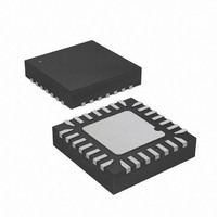
ATTINY88-MMHR Atmel, ATTINY88-MMHR Datasheet - Page 3

ATTINY88-MMHR
Manufacturer Part Number
ATTINY88-MMHR
Description
MCU AVR 8KB FLASH 12MHZ 28QFN
Manufacturer
Atmel
Series
AVR® ATtinyr
Datasheet
1.ATTINY48-MU.pdf
(302 pages)
Specifications of ATTINY88-MMHR
Core Processor
AVR
Core Size
8-Bit
Speed
12MHz
Connectivity
I²C, SPI
Peripherals
Brown-out Detect/Reset, POR, WDT
Number Of I /o
24
Program Memory Size
8KB (4K x 16)
Program Memory Type
FLASH
Eeprom Size
64 x 8
Ram Size
512 x 8
Voltage - Supply (vcc/vdd)
1.8 V ~ 5.5 V
Data Converters
A/D 8x10b
Oscillator Type
Internal
Operating Temperature
-40°C ~ 85°C
Package / Case
*
Lead Free Status / RoHS Status
Lead free / RoHS Compliant
- Current page: 3 of 302
- Download datasheet (9Mb)
1.1
1.1.1
1.1.2
1.1.3
1.1.4
1.1.5
1.1.6
1.1.7
8008G–AVR–04/11
Pin Descriptions
VCC
AVCC
GND
Port A (PA3:0)
Port B (PB7:0)
Port C (PC7, PC5:0)
PC6/RESET
Digital supply voltage.
AV
be externally connected to V
mended this pin is connected to V
Canceling Techniques” on page
The following pins receive their supply voltage from AV
ages) PA[1:0]. All other I/O pins take their supply voltage from V
Ground.
Port A is a 4-bit bi-directional I/O port with internal pull-up resistors (selected for each bit). The
PA[3:0] output buffers have symmetrical drive characteristics with both sink and source capabil-
ity. As inputs, Port A pins that are externally pulled low will source current if the pull-up resistors
are activated. The Port A pins are tri-stated when a reset condition becomes active, even if the
clock is not running.
This port is available in 32-lead TQFP, 32-pad QFN and 32-ball UFBGA packages, only.
Port B is an 8-bit bi-directional I/O port with internal pull-up resistors (selected for each bit). The
Port B output buffers have symmetrical drive characteristics with both sink and source capability.
As inputs, Port B pins that are externally pulled low will source current if the pull-up resistors are
activated. The Port B pins are tri-stated when a reset condition becomes active, even if the clock
is not running.
Depending on the clock selection fuse settings, PB6 can be used as input to the internal clock
operating circuit.
The various special features of Port B are elaborated in
69.
Port C is a 8-bit bi-directional I/O port with internal pull-up resistors (selected for each bit). The
PC7 and PC[5:0] output buffers have symmetrical drive characteristics with both sink and source
capability. As inputs, Port C pins that are externally pulled low will source current if the pull-up
resistors are activated. The Port C pins are tri-stated when a reset condition becomes active,
even if the clock is not running.
If the RSTDISBL Fuse is programmed, PC6 is used as an I/O pin. Note that the electrical char-
acteristics of PC6 differ from those of the other pins of Port C.
If the RSTDISBL Fuse is unprogrammed, PC6 is used as a reset input. A low level on this pin for
longer than the minimum pulse width will generate a reset, even if the clock is not running. The
CC
is the supply voltage pin for the A/D converter and a selection of I/O pins. This pin should
CC
172.
even if the ADC is not used. If the ADC is used, it is recom-
CC
through a low-pass filter, as described in
CC
“Alternate Functions of Port B” on page
: PC7, PC[5:0] and (in 32-lead pack-
CC
.
ATtiny48/88
“Analog Noise
3
Related parts for ATTINY88-MMHR
Image
Part Number
Description
Manufacturer
Datasheet
Request
R

Part Number:
Description:
Manufacturer:
Atmel Corporation
Datasheet:

Part Number:
Description:
Manufacturer:
Atmel Corporation
Datasheet:

Part Number:
Description:
MCU AVR 8K ISP FLASH 1.8V 32TQFP
Manufacturer:
Atmel
Datasheet:

Part Number:
Description:
MCU AVR 8K FLASH 12MHZ 28-QFN
Manufacturer:
Atmel
Datasheet:

Part Number:
Description:
MCU AVR 8KB FLASH 12MHZ 28-VQFN
Manufacturer:
Atmel
Datasheet:

Part Number:
Description:
IC MCU AVR 8B 8KB FLASH 32QFN
Manufacturer:
Atmel
Datasheet:

Part Number:
Description:
MCU AVR 8K ISP FLASH 1.8V 32-QFN
Manufacturer:
Atmel
Datasheet:

Part Number:
Description:
MCU AVR 8K ISP FLASH 1.8V 28-DIP
Manufacturer:
Atmel
Datasheet:

Part Number:
Description:
MCU AVR 8KB FLASH 12MHZ 32TQFP
Manufacturer:
Atmel
Datasheet:

Part Number:
Description:
MCU AVR 8KB FLASH 12MHZ 32QFN
Manufacturer:
Atmel
Datasheet:

Part Number:
Description:
MCU AVR 8KB FLASH 12MHZ 32QFN
Manufacturer:
Atmel
Datasheet:

Part Number:
Description:
8-bit Microcontrollers - MCU Microcontroller
Manufacturer:
Atmel

Part Number:
Description:
8-bit Microcontrollers - MCU Microcontroller
Manufacturer:
Atmel


