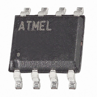
ATTINY13A-SU Atmel, ATTINY13A-SU Datasheet - Page 92

ATTINY13A-SU
Manufacturer Part Number
ATTINY13A-SU
Description
IC MCU AVR 1K FLASH 20MHZ 8SOIC
Manufacturer
Atmel
Series
AVR® ATtinyr
Specifications of ATTINY13A-SU
Core Processor
AVR
Core Size
8-Bit
Speed
20MHz
Peripherals
Brown-out Detect/Reset, POR, PWM, WDT
Number Of I /o
6
Program Memory Size
1KB (512 x 16)
Program Memory Type
FLASH
Eeprom Size
64 x 8
Ram Size
64 x 8
Voltage - Supply (vcc/vdd)
1.8 V ~ 5.5 V
Data Converters
A/D 4x10b
Oscillator Type
Internal
Operating Temperature
-40°C ~ 85°C
Package / Case
8-SOIC (5.3mm Width), 8-SOP, 8-SOEIAJ
Cpu Family
ATtiny
Device Core
AVR
Device Core Size
8b
Frequency (max)
20MHz
Interface Type
SPI
Total Internal Ram Size
64Byte
# I/os (max)
6
Number Of Timers - General Purpose
1
Operating Supply Voltage (typ)
2.5/3.3/5V
Operating Supply Voltage (max)
5.5V
Operating Supply Voltage (min)
1.8V
On-chip Adc
4-chx10-bit
Instruction Set Architecture
RISC
Operating Temp Range
-40C to 85C
Operating Temperature Classification
Industrial
Mounting
Surface Mount
Pin Count
8
Package Type
SOIC EIAJ
Processor Series
ATTINY1x
Core
AVR8
Data Bus Width
8 bit
Data Ram Size
64 B
Maximum Clock Frequency
20 MHz
Number Of Programmable I/os
6
Number Of Timers
1
Maximum Operating Temperature
+ 85 C
Mounting Style
SMD/SMT
3rd Party Development Tools
EWAVR, EWAVR-BL
Development Tools By Supplier
ATAVRDRAGON, ATSTK500, ATSTK600, ATAVRISP2, ATAVRONEKIT, ATAKSTK511
Minimum Operating Temperature
- 40 C
Package
8SOIC EIAJ
Family Name
ATtiny
Maximum Speed
20 MHz
Operating Supply Voltage
2.5|3.3|5 V
For Use With
ATSTK600-DIP40 - STK600 SOCKET/ADAPTER 40-PDIP770-1007 - ISP 4PORT ATMEL AVR MCU SPI/JTAG770-1004 - ISP 4PORT FOR ATMEL AVR MCU SPIATAVRDRAGON - KIT DRAGON 32KB FLASH MEM AVRATAVRISP2 - PROGRAMMER AVR IN SYSTEMATJTAGICE2 - AVR ON-CHIP D-BUG SYSTEM
Lead Free Status / RoHS Status
Lead free / RoHS Compliant
Connectivity
-
Lead Free Status / Rohs Status
Compliant
Available stocks
Company
Part Number
Manufacturer
Quantity
Price
Company:
Part Number:
ATTINY13A-SU
Manufacturer:
TI
Quantity:
21 550
Part Number:
ATTINY13A-SU
Manufacturer:
ATMEL/爱特梅尔
Quantity:
20 000
14.11 ADC Conversion Result
14.12 Register Description
14.12.1
92
ATtiny13A
ADMUX – ADC Multiplexer Selection Register
After the conversion is complete (ADIF is high), the conversion result can be found in the ADC
Result Registers (ADCL, ADCH).
For single ended conversion, the result is
where V
Table 14-2 on page 92
0x3FF represents the selected reference voltage minus one LSB.
• Bits 7, 4:2 – Res: Reserved Bits
These bits are reserved bits in the ATtiny13A and will always read as zero.
• Bit 6 – REFS0: Reference Selection Bit
This bit selects the voltage reference for the ADC, as shown in
during a conversion, the change will not go in effect until this conversion is complete (ADIF in
ADCSRA is set).
Table 14-2.
• Bit 5 – ADLAR: ADC Left Adjust Result
The ADLAR bit affects the presentation of the ADC conversion result in the ADC Data Register.
Write one to ADLAR to left adjust the result. Otherwise, the result is right adjusted. Changing the
ADLAR bit will affect the ADC Data Register immediately, regardless of any ongoing conver-
sions. For a complete description of this bit, see
page
Bit
0x07
Read/Write
Initial Value
• Quantization Error: Due to the quantization of the input voltage into a finite number of codes,
• Absolute Accuracy: The maximum deviation of an actual (unadjusted) transition compared to
a range of input voltages (1 LSB wide) will code to the same value. Always ± 0.5 LSB.
an ideal transition for any code. This is the compound effect of offset, gain error, differential
error, non-linearity, and quantization error. Ideal value: ± 0.5 LSB.
94.
IN
is the voltage on the selected input pin and V
REFS0
Voltage Reference Selections for ADC
0
1
R
7
–
0
REFS0
and
R/W
6
0
Table 14-3 on page
ADLAR
Voltage Reference Selection
V
Internal Voltage Reference.
R/W
CC
5
0
used as analog reference.
ADC
=
R
4
–
0
V
--------------------------
IN
“ADCL and ADCH – The ADC Data Register” on
V
⋅
REF
1024
93). 0x000 represents analog ground, and
R
3
–
0
REF
the selected voltage reference (see
R
2
–
0
Table
MUX1
14-2. If this bit is changed
R/W
1
0
MUX0
R/W
0
0
8126E–AVR–07/10
ADMUX


