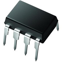
PIC12C672-10E/P Microchip Technology, PIC12C672-10E/P Datasheet - Page 365

PIC12C672-10E/P
Manufacturer Part Number
PIC12C672-10E/P
Description
IC MCU OTP 2KX14 A/D 8DIP
Manufacturer
Microchip Technology
Series
PIC® 12Cr
Datasheets
1.PIC16F688T-ISL.pdf
(688 pages)
2.PIC12CE673-10P.pdf
(129 pages)
3.PIC12CE673-10P.pdf
(14 pages)
Specifications of PIC12C672-10E/P
Core Processor
PIC
Core Size
8-Bit
Speed
10MHz
Peripherals
POR, WDT
Number Of I /o
5
Program Memory Size
3.5KB (2K x 14)
Program Memory Type
OTP
Ram Size
128 x 8
Voltage - Supply (vcc/vdd)
3 V ~ 5.5 V
Data Converters
A/D 4x8b
Oscillator Type
Internal
Operating Temperature
-40°C ~ 125°C
Package / Case
8-DIP (0.300", 7.62mm)
Processor Series
PIC12C
Core
PIC
Data Bus Width
8 bit
Data Ram Size
128 B
Maximum Clock Frequency
10 MHz
Number Of Programmable I/os
5
Number Of Timers
8
Maximum Operating Temperature
+ 125 C
Mounting Style
Through Hole
3rd Party Development Tools
52715-96, 52716-328, 52717-734
Development Tools By Supplier
ICE2000
Minimum Operating Temperature
- 40 C
On-chip Adc
8
Data Rom Size
128 B
Height
3.3 mm
Length
9.27 mm
Supply Voltage (max)
5.5 V
Supply Voltage (min)
3 V
Width
6.35 mm
Lead Free Status / RoHS Status
Lead free / RoHS Compliant
Eeprom Size
-
Connectivity
-
Lead Free Status / Rohs Status
Details
- Current page: 365 of 688
- Download datasheet (3Mb)
19.4
19.5
19.6
1997 Microchip Technology Inc.
Voltage Reference Accuracy/Error
Operation During Sleep
Effects of a Reset
The full range of V
sistors on the top and bottom of the resistor ladder network
approaching V
changes with fluctuations in V
in the Device Data Sheets electrical specification
When the device wakes up from sleep through an interrupt or a Watchdog Timer time-out, the
contents of the VRCON register are not affected. To minimize current consumption in SLEEP
mode, the Voltage Reference should be disabled.
A device reset disables the Voltage Reference by clearing the VREN bit (VRCON<7>). This reset
also disconnects the reference from the V
selects the high voltage range by clearing the VRR bit (VRCON<5>). The V
VRCON<3:0>, are also cleared.
SS
Section 19. Voltage Reference
or V
SS
to V
DD
. The Voltage Reference is V
DD
cannot be realized due to the construction of the module. The tran-
DD
. The absolute accuracy of the Voltage Reference can be found
REF
pin by clearing the VROE bit (VRCON<6>) and
parameter
DD
derived and therefore, the V
D311.
(Figure
19-1) keep V
REF
DS31019A-page 19-5
value select bits,
REF
REF
output
from
19
Related parts for PIC12C672-10E/P
Image
Part Number
Description
Manufacturer
Datasheet
Request
R

Part Number:
Description:
IC MCU OTP 2KX14 A/D 8DIP
Manufacturer:
Microchip Technology
Datasheet:

Part Number:
Description:
IC MCU OTP 2KX14 A/D 8-SOIJ
Manufacturer:
Microchip Technology
Datasheet:

Part Number:
Description:
IC MCU OTP 2KX14 A/D 8-SOIJ
Manufacturer:
Microchip Technology
Datasheet:

Part Number:
Description:
IC MCU OTP 2KX14 A/D 8-SOIJ
Manufacturer:
Microchip Technology
Datasheet:

Part Number:
Description:
IC MCU OTP 2KX14 A/D 8DIP
Manufacturer:
Microchip Technology
Datasheet:

Part Number:
Description:
IC MCU OTP 2KX14 A/D 8-SOIJ
Manufacturer:
Microchip Technology
Datasheet:

Part Number:
Description:
IC MCU OTP 2KX14 A/D 8DFN
Manufacturer:
Microchip Technology
Datasheet:

Part Number:
Description:
IC PIC MCU 2KX14 8DFN
Manufacturer:
Microchip Technology
Datasheet:

Part Number:
Description:
IC MCU OTP 2KX14 A/D 8-SOIJ
Manufacturer:
Microchip Technology
Datasheet:

Part Number:
Description:
IC MCU OTP 2KX14 A/D 8DFN
Manufacturer:
Microchip Technology
Datasheet:

Part Number:
Description:
IC MCU OTP 2KX14 A/D 8DIP
Manufacturer:
Microchip Technology
Datasheet:

Part Number:
Description:
IC MCU OTP 2KX14 A/D 8-SOIJ
Manufacturer:
Microchip Technology
Datasheet:

Part Number:
Description:
IC MCU EPROM 2KX14 A/D 8CDIP
Manufacturer:
Microchip Technology
Datasheet:

Part Number:
Description:
IC,MICROCONTROLLER,8-BIT,PIC CPU,CMOS,DIP,8PIN,PLASTIC
Manufacturer:
Microchip Technology
Datasheet:

Part Number:
Description:
IC,MICROCONTROLLER,8-BIT,PIC CPU,CMOS,DIP,8PIN,PLASTIC
Manufacturer:
Microchip Technology
Datasheet:


