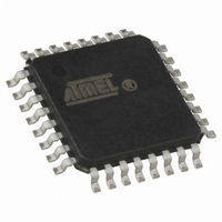
ATTINY28L-4AU Atmel, ATTINY28L-4AU Datasheet - Page 2

ATTINY28L-4AU
Manufacturer Part Number
ATTINY28L-4AU
Description
IC MCU AVR 2K FLASH 4MHZ 32-TQFP
Manufacturer
Atmel
Series
AVR® ATtinyr
Specifications of ATTINY28L-4AU
Core Processor
AVR
Core Size
8-Bit
Speed
4MHz
Peripherals
POR, WDT
Number Of I /o
11
Program Memory Size
2KB (1K x 16)
Program Memory Type
FLASH
Voltage - Supply (vcc/vdd)
2.7 V ~ 5.5 V
Oscillator Type
Internal
Operating Temperature
-40°C ~ 85°C
Package / Case
32-TQFP, 32-VQFP
Processor Series
ATTINY2x
Core
AVR8
Data Bus Width
8 bit
Data Ram Size
32 B
Maximum Clock Frequency
4 MHz
Number Of Programmable I/os
11
Number Of Timers
1
Maximum Operating Temperature
+ 85 C
Mounting Style
SMD/SMT
3rd Party Development Tools
EWAVR, EWAVR-BL
Development Tools By Supplier
ATAVRDRAGON, ATSTK500, ATSTK600, ATAVRISP2, ATAVRONEKIT
Minimum Operating Temperature
- 40 C
On-chip Adc
8 bit
Package
32TQFP
Device Core
AVR
Family Name
ATtiny
Maximum Speed
4 MHz
Ram Size
32 Byte
Operating Supply Voltage
3.3|5 V
For Use With
ATSTK600-DIP40 - STK600 SOCKET/ADAPTER 40-PDIPATSTK500 - PROGRAMMER AVR STARTER KIT
Lead Free Status / RoHS Status
Lead free / RoHS Compliant
Eeprom Size
-
Ram Size
-
Data Converters
-
Connectivity
-
Lead Free Status / Rohs Status
Details
Available stocks
Company
Part Number
Manufacturer
Quantity
Price
Description
Block Diagram
2
ATtiny28L/V
The ATtiny28 is a low-power CMOS 8-bit microcontroller based on the AVR RISC archi-
tecture. By executing powerful instructions in a single clock cycle, the ATtiny28 achieves
throughputs approaching 1 MIPS per MHz, allowing the system designer to optimize
power consumption versus processing speed. The AVR core combines a rich instruction
set with 32 general-purpose working registers. All the 32 registers are directly con-
nected to the Arithmetic Logic Unit (ALU), allowing two independent registers to be
accessed in one single instruction executed in one clock cycle. The resulting architec-
ture is more code efficient while achieving throughputs up to ten times faster than
conventional CISC microcontrollers.
Figure 1. The ATtiny28 Block Diagram
The ATtiny28 provides the following features: 2K bytes of Flash, 11 general-purpose I/O
lines, 8 input lines, a high-current LED driver, 32 general-purpose working registers, an
8-bit timer/counter, internal and external interrupts, programmable Watchdog Timer with
internal oscillator and 2 software-selectable power-saving modes. The Idle Mode stops
the CPU while allowing the timer/counter and interrupt system to continue functioning.
The Power-down mode saves the register contents but freezes the oscillator, disabling
all other chip functions until the next interrupt or hardware reset. The wake-up or inter-
GND
VCC
PROGRAMMING
INSTRUCTION
INSTRUCTION
CONTROL
PROGRAM
COUNTER
PROGRAM
REGISTER
DECODER
LINES
FLASH
LOGIC
DATA REGISTER
PORTB
PORTB
HARDWARE
REGISTERS
REGISTER
GENERAL
PURPOSE
POINTER
STATUS
STACK
STACK
ALU
Z
8-BIT DATA BUS
DATA REGISTER
PORTD
MCU CONTROL
OSCILLATOR
WATCHDOG
INTERRUPT
COUNTER
REGISTER
INTERNAL
TIMER/
TIMER
UNIT
PORTD
XTAL1
REG. PORTD
DATA DIR
OSCILLATOR
TIMING AND
CONTROL
XTAL2
DATA REGISTER
CALIBRATED
OSCILLATOR
PORTA
INTERNAL
MODULATOR
PORTA
HARDWARE
PORTA CONTROL
REGISTER
1062FS–AVR–07/06
RESET


