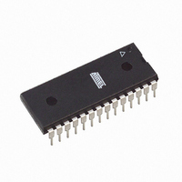
ATMEGA8L-8PU Atmel, ATMEGA8L-8PU Datasheet - Page 115

ATMEGA8L-8PU
Manufacturer Part Number
ATMEGA8L-8PU
Description
IC AVR MCU 8K 8MHZ 3V 28DIP
Manufacturer
Atmel
Series
AVR® ATmegar
Datasheets
1.ATMEGA8L-8MU.pdf
(25 pages)
2.ATMEGA8L-8MU.pdf
(302 pages)
3.ATMEGA8-16PU.pdf
(305 pages)
Specifications of ATMEGA8L-8PU
Core Processor
AVR
Core Size
8-Bit
Speed
8MHz
Connectivity
I²C, SPI, UART/USART
Peripherals
Brown-out Detect/Reset, POR, PWM, WDT
Number Of I /o
23
Program Memory Size
8KB (4K x 16)
Program Memory Type
FLASH
Eeprom Size
512 x 8
Ram Size
1K x 8
Voltage - Supply (vcc/vdd)
2.7 V ~ 5.5 V
Data Converters
A/D 6x10b
Oscillator Type
Internal
Operating Temperature
-40°C ~ 85°C
Package / Case
28-DIP (0.300", 7.62mm)
Cpu Family
ATmega
Device Core
AVR
Device Core Size
8b
Frequency (max)
8MHz
Interface Type
SPI/TWI/USART
Total Internal Ram Size
1KB
# I/os (max)
23
Number Of Timers - General Purpose
3
Operating Supply Voltage (typ)
3.3/5V
Operating Supply Voltage (max)
5.5V
Operating Supply Voltage (min)
2.7V
On-chip Adc
6-chx10-bit
Instruction Set Architecture
RISC
Operating Temp Range
-40C to 85C
Operating Temperature Classification
Industrial
Mounting
Through Hole
Pin Count
28
Package Type
PDIP
Processor Series
ATMEGA8x
Core
AVR8
Data Bus Width
8 bit
Data Ram Size
1 KB
Maximum Clock Frequency
8 MHz
Number Of Programmable I/os
23
Number Of Timers
3
Operating Supply Voltage
2.7 V to 5.5 V
Maximum Operating Temperature
+ 85 C
Mounting Style
Through Hole
3rd Party Development Tools
EWAVR, EWAVR-BL
Minimum Operating Temperature
- 40 C
Controller Family/series
AVR MEGA
No. Of I/o's
23
Eeprom Memory Size
512Byte
Ram Memory Size
1KB
Cpu Speed
8MHz
Rohs Compliant
Yes
For Use With
ATSTK600-TQFP32 - STK600 SOCKET/ADAPTER 32-TQFPATSTK600-DIP40 - STK600 SOCKET/ADAPTER 40-PDIP770-1007 - ISP 4PORT ATMEL AVR MCU SPI/JTAGATAVRISP2 - PROGRAMMER AVR IN SYSTEMATSTK500 - PROGRAMMER AVR STARTER KIT
Lead Free Status / RoHS Status
Lead free / RoHS Compliant
Available stocks
Company
Part Number
Manufacturer
Quantity
Price
Company:
Part Number:
ATMEGA8L-8PU
Manufacturer:
BROADCOM
Quantity:
101
Company:
Part Number:
ATMEGA8L-8PU
Manufacturer:
ATMEL
Quantity:
33 600
Part Number:
ATMEGA8L-8PU
Manufacturer:
ATMEL/爱特梅尔
Quantity:
20 000
Company:
Part Number:
ATMEGA8L-8PU-QS096
Manufacturer:
ATMEL
Quantity:
56
8-bit Timer/Counter
Register Description
Timer/Counter Control
Register – TCCR2
2486O–AVR–10/04
• Bit 7 – FOC2: Force Output Compare
The FOC2 bit is only active when the WGM bits specify a non-PWM mode. However, for
ensuring compatibility with future devices, this bit must be set to zero when TCCR2 is
written when operating in PWM mode. When writing a logical one to the FOC2 bit, an
immediate Compare Match is forced on the waveform generation unit. The OC2 output
is changed according to its COM21:0 bits setting. Note that the FOC2 bit is implemented
as a strobe. Therefore it is the value present in the COM21:0 bits that determines the
effect of the forced compare.
A FOC2 strobe will not generate any interrupt, nor will it clear the timer in CTC mode
using OCR2 as TOP.
The FOC2 bit is always read as zero.
• Bit 6,3 – WGM21:0: Waveform Generation Mode
These bits control the counting sequence of the counter, the source for the maximum
(TOP) counter value, and what type of waveform generation to be used. Modes of oper-
ation supported by the Timer/Counter unit are: Normal mode, Clear Timer on Compare
Match (CTC) mode, and two types of Pulse Width Modulation (PWM) modes. See Table
42 and “Modes of Operation” on page 108.
Table 42. Waveform Generation Mode Bit Description
Note:
• Bit 5:4 – COM21:0: Compare Match Output Mode
These bits control the Output Compare Pin (OC2) behavior. If one or both of the
COM21:0 bits are set, the OC2 output overrides the normal port functionality of the I/O
pin it is connected to. However, note that the Data Direction Register (DDR) bit corre-
sponding to OC2 pin must be set in order to enable the output driver.
When OC2 is connected to the pin, the function of the COM21:0 bits depends on the
WGM21:0 bit setting. Table 43 shows the COM21:0 bit functionality when the WGM21:0
bits are set to a normal or CTC mode (non-PWM).
Bit
Read/Write
Initial Value
Mode
0
1
2
3
1. The CTC2 and PWM2 bit definition names are now obsolete. Use the WGM21:0 def-
WGM21
(CTC2)
initions. However, the functionality and location of these bits are compatible with
previous versions of the timer.
0
0
1
1
FOC2
W
7
0
WGM20
(PWM2)
WGM20
R/W
0
1
0
1
6
0
COM21
Timer/Counter Mode
of Operation
Normal
PWM, Phase Correct
CTC
Fast PWM
R/W
5
0
COM20
R/W
4
0
(1)
WGM21
R/W
3
0
TOP
0xFF
0xFF
OCR2
0xFF
CS22
R/W
2
0
Update of
OCR2
Immediate
TOP
Immediate
TOP
CS21
ATmega8(L)
R/W
1
0
CS20
R/W
0
0
TOV2 Flag
Set
MAX
BOTTOM
MAX
MAX
TCCR2
115


