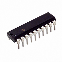
PIC16C781-I/P Microchip Technology, PIC16C781-I/P Datasheet - Page 75

PIC16C781-I/P
Manufacturer Part Number
PIC16C781-I/P
Description
IC MCU OTP 1KX14 W/AD COMP 20DIP
Manufacturer
Microchip Technology
Series
PIC® 16Cr
Datasheets
1.PIC16C781-ISO.pdf
(186 pages)
2.PIC16C781-ISO.pdf
(8 pages)
3.PIC16C781-ISO.pdf
(8 pages)
Specifications of PIC16C781-I/P
Core Size
8-Bit
Program Memory Size
1.75KB (1K x 14)
Core Processor
PIC
Speed
20MHz
Peripherals
Brown-out Detect/Reset, POR, PWM, WDT
Number Of I /o
13
Program Memory Type
OTP
Ram Size
128 x 8
Voltage - Supply (vcc/vdd)
4 V ~ 5.5 V
Data Converters
A/D 8x8b; D/A 1x8b
Oscillator Type
Internal
Operating Temperature
-40°C ~ 85°C
Package / Case
20-DIP (0.300", 7.62mm)
Controller Family/series
PIC16C
No. Of I/o's
16
Ram Memory Size
128Byte
Cpu Speed
20MHz
No. Of Timers
3
Processor Series
PIC16C
Core
PIC
Data Bus Width
8 bit
Data Ram Size
128 B
Maximum Clock Frequency
20 MHz
Number Of Programmable I/os
16
Number Of Timers
2
Operating Supply Voltage
2.5 V to 5.5 V
Maximum Operating Temperature
+ 85 C
Mounting Style
Through Hole
3rd Party Development Tools
52715-96, 52716-328, 52717-734
Development Tools By Supplier
ICE2000, DM163022
Minimum Operating Temperature
- 40 C
On-chip Adc
8 bit
On-chip Dac
8 bit, 1 Channel
Lead Free Status / RoHS Status
Lead free / RoHS Compliant
For Use With
ISPICR1 - ADAPTER IN-CIRCUIT PROGRAMMINGDVA16XP202 - ADAPTER DEVICE PIC16C781/782DM163012 - BOARD DEMO PICDEM FOR 16C781/782AC164028 - MODULE SKT PROMATEII 20SOIC/DIP
Eeprom Size
-
Connectivity
-
Lead Free Status / Rohs Status
Details
Other names
PIC16C781I/P
9.2.4
The Analog-to-Digital conversion is initiated by setting
the GO/DONE bit in ADCON0 register. When the con-
version is complete, the ADC module:
• Clears the GO/DONE bit
• Sets the ADIF flag in the PIR1 register
• Generates an interrupt if the ADIE, PEIE, and GIE
If the conversion must be aborted, the GO/DONE bit
can be cleared in software. The ADRES register will not
be updated with the partially completed ADC conver-
sion sample. Instead, the ADRES will contain the value
from the last completed conversion. After an aborted
conversion, a 2T
acquisition/conversion can be initiated. Following the
delay, an input acquisition is automatically started on
the selected channel.
9.3
For the ADC module to meet its specified accuracy, the
internal Sample-and-Hold capacitor (C
allowed to charge to within ½ LSb of the voltage present
on the input channel (see analog input model in Figure
9-2). The analog source resistance (R
sampling switch resistance (R
time required to charge C
over the power supply voltage range (AV
affect the input offset voltage at the analog input (due to
pin leakage current). Therefore:
1.
2.
To calculate the minimum acquisition time, Equation 9-1
may be used. This equation calculates the acquisition
time to within ½ LSb error, assuming an 8-bit conver-
sion (512 steps for the PIC16C781/782 ADC). The ½
LSb error is the maximum error allowed for the ADC to
meet its specified accuracy.
EQUATION 9-1:
V
Given: V
The above equation reduces to:
T
bits are set.
Note:
CAP
2001 Microchip Technology Inc.
HOLD
The maximum recommended impedance for
any analog sources is 10 kOhms.
Following any change in the analog input chan-
nel selection, a minimum acquisition delay must
be observed before another conversion can
begin (see Equation 9-1).
= -(51.2 pF)(1 k + R
= (ADC
HOLD
ADC Acquisition Requirements
The GO/DONE bit should NOT be set in
the same instruction that turns on the ADC.
INITIATING A CONVERSION
= (ADC
REF
-(ADC
AD
REF
delay is required before another
REF
ADC MINIMUM
CHARGING TIME
/512), for 1/2LSb resolution
SS
HOLD
/512))•(1-e
+ R
S
SS
. In addition, R
) Ln(1/511)
) will directly affect the
-T
CAP
S
) and the internal
/C
HOLD
DD
HOLD
), and R
(R
SS
) must be
IC
+Rss+Rs)
will vary
S
Preliminary
will
)
Example 9-1 shows the calculation of the minimum
required acquisition time T
based on the following system assumptions.
C
R
1/2 LSb error
R
EXAMPLE 9-1:
HOLD
S
SS
T
T
T
T
ACQ
ACQ
CAP
ACQ
Note 1: The reference voltage (ADC
= 10k
= 7k @ V
= 51.2 pF
= Amplifier Setting Time +
= 5 s + T
= -C
= 5 s + 5.747 s + [(50 C -25 C)(0.05 s/ C)]
2: The charge holding capacitor (C
3: The maximum recommended impedance
4: After a conversion has completed, a
Holding Capacitor Charging Time +
Temperature Coefficient
-51.2 pF (1
-51.2 pF (18
-0.921 s (-6.2364)
5.747 s
10.747 s + 1.25 s
11.997 s
effect on the equation, since it cancels
itself out.
not discharged after each conversion.
for analog sources is 10
required to meet the pin leakage specifi-
cation.
1.0T
acquisition can begin again. During this
time the holding capacitor is not connected
to the selected ADC input channel.
HOLD
PIC16C781/782
DD
AD
= 5V
CAP
(R
delay must be completed before
IC
CALCULATING THE
MINIMUM REQUIRED
ACQUISITION TIME
k
+ [(Temp - 25 C)(0.05 s/ C)]
k
+ R
+ 7
) In(0.0020)
SS
ACQ
k
+ R
+ 10
. This calculation is
S
) In(1/511)
DS41171A-page 73
k
In(0.0020)
k
REF
) has no
HOLD
This is
) is


