PIC18LF47J53-I/ML Microchip Technology, PIC18LF47J53-I/ML Datasheet - Page 299
PIC18LF47J53-I/ML
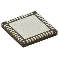
Manufacturer Part Number
PIC18LF47J53-I/ML
Description
IC PIC MCU 128KB FLASH 44QFN
Manufacturer
Microchip Technology
Series
PIC® XLP™ 18Fr
Datasheets
1.PIC18LF24J10-ISS.pdf
(32 pages)
2.PIC18F26J13-ISS.pdf
(496 pages)
3.PIC18F26J53-ISS.pdf
(586 pages)
4.PIC18F26J53-ISS.pdf
(12 pages)
Specifications of PIC18LF47J53-I/ML
Core Size
8-Bit
Program Memory Size
128KB (64K x 16)
Core Processor
PIC
Speed
48MHz
Connectivity
I²C, LIN, SPI, UART/USART, USB
Peripherals
Brown-out Detect/Reset, POR, PWM, WDT
Number Of I /o
34
Program Memory Type
FLASH
Ram Size
3.8K x 8
Voltage - Supply (vcc/vdd)
2 V ~ 2.75 V
Data Converters
A/D 13x10b/12b
Oscillator Type
Internal
Operating Temperature
-40°C ~ 85°C
Package / Case
*
Controller Family/series
PIC18
Cpu Speed
48MHz
Digital Ic Case Style
QFN
Supply Voltage Range
1.8V To 3.6V
Embedded Interface Type
I2C, SPI, USART
Rohs Compliant
Yes
Lead Free Status / RoHS Status
Lead free / RoHS Compliant
Eeprom Size
-
Lead Free Status / RoHS Status
Lead free / RoHS Compliant, Lead free / RoHS Compliant


REGISTER 17-1:
REGISTER 17-2:
2010 Microchip Technology Inc.
bit 0
Note 1:
bit 7
Legend:
R = Readable bit
-n = Value at POR
bit 7
bit 6-4
bit 3-2
bit 1-0
TRIGSEL
R/W-0
2:
Available on PIC18(L)F4XK22 devices only.
Allow greater than 15 s acquisition time when measuring the Fixed Voltage Reference.
ADON: ADC Enable bit
1 = ADC is enabled
0 = ADC is disabled and consumes no operating current
TRIGSEL: Special Trigger Select bit
1 = Selects the special trigger from CTMU
0 = Selects the special trigger from CCP5
Unimplemented: Read as ‘0’
PVCFG<1:0>: Positive Voltage Reference Configuration bits
00 = A/D V
01 = A/D V
10 = A/D V
11 = Reserved (by default, A/D V
NVCFG0<1:0>: Negative Voltage Reference Configuration bits
00 = A/D V
01 = A/D V
10 = Reserved (by default, A/D V
11 = Reserved (by default, A/D V
U-0
—
ADCON0: A/D CONTROL REGISTER 0 (CONTINUED)
ADCON1: A/D CONTROL REGISTER 1
REF
REF
REF
REF
REF
W = Writable bit
‘1’ = Bit is set
+ connected to internal signal, AV
+ connected to external pin, V
+ connected to internal signal, FVR BUF2
- connected to internal signal, AV
- connected to external pin, V
U-0
—
REF
REF
REF
U-0
—
Preliminary
+ connected to internal signal, AV
+ connected to internal signal, AV
+ connected to internal signal, AV
U = Unimplemented bit, read as ‘0’
‘0’ = Bit is cleared
REF
REF
R/W-0
-
SS
+
DD
PIC18(L)F2X/4XK22
PVCFG<1:0>
R/W-0
DD
SS
SS
x = Bit is unknown
)
)
)
R/W-0
NVCFG<1:0>
DS41412D-page 299
R/W-0
bit 0
Related parts for PIC18LF47J53-I/ML
Image
Part Number
Description
Manufacturer
Datasheet
Request
R

Part Number:
Description:
Manufacturer:
Microchip Technology Inc.
Datasheet:
Part Number:
Description:
Manufacturer:
Microchip Technology Inc.
Datasheet:
Part Number:
Description:
Manufacturer:
Microchip Technology Inc.
Datasheet:
Part Number:
Description:
Manufacturer:
Microchip Technology Inc.
Datasheet:
Part Number:
Description:
Manufacturer:
Microchip Technology Inc.
Datasheet:
Part Number:
Description:
Manufacturer:
Microchip Technology Inc.
Datasheet:
Part Number:
Description:
Manufacturer:
Microchip Technology Inc.
Datasheet:
Part Number:
Description:
Manufacturer:
Microchip Technology Inc.
Datasheet: