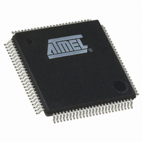
AT91M40800-33AU-999 Atmel, AT91M40800-33AU-999 Datasheet - Page 7

AT91M40800-33AU-999
Manufacturer Part Number
AT91M40800-33AU-999
Description
IC MCU 32BIT RISC 100LQFP
Manufacturer
Atmel
Series
AT91SAMr
Datasheet
1.AT91M40800-33AU.pdf
(18 pages)
Specifications of AT91M40800-33AU-999
Core Processor
ARM7
Core Size
16/32-Bit
Speed
33MHz
Connectivity
EBI/EMI, UART/USART
Peripherals
POR, WDT
Number Of I /o
32
Program Memory Type
ROMless
Ram Size
8K x 8
Voltage - Supply (vcc/vdd)
1.8 V ~ 3.6 V
Oscillator Type
External
Operating Temperature
-40°C ~ 85°C
Package / Case
100-LQFP
Processor Series
AT91Mx
Core
ARM7TDMI
Data Bus Width
32 bit
Data Ram Size
8 KB
Interface Type
EBI, USART
Maximum Clock Frequency
66 MHz
Number Of Programmable I/os
32
Number Of Timers
3
Maximum Operating Temperature
+ 85 C
3rd Party Development Tools
JTRACE-ARM-2M, MDK-ARM, RL-ARM, ULINK2
Minimum Operating Temperature
- 40 C
Lead Free Status / RoHS Status
Lead free / RoHS Compliant
Eeprom Size
-
Program Memory Size
-
Data Converters
-
Lead Free Status / Rohs Status
Details
Available stocks
Company
Part Number
Manufacturer
Quantity
Price
7. Product Overview
7.1
7.2
7.3
7.4
7.4.1
7.4.2
7.5
7.5.1
1348FS–ATARM–13-Apr-06
Power Supply
Input/Output Considerations
Master Clock
Reset
Emulation Functions
NRST Pin
Watchdog Reset
Tri-state Mode
The AT91M40800 microcontroller has a unique type of power supply pin – VDD. The VDD pin
supplies the I/O pads and the device core. The supported voltage range on V
The AT91M40800 microcontroller I/O pads are 5V-tolerant, enabling them to interface with
external 5V devices without any additional components. Thus, the devices accept 5V (3V) on the
inputs even if powered at 3V (2V). For further information, refer to the “AT91M40800 Electrical
Characteristics” datasheet.
After the reset, the peripheral I/Os are initialized as inputs to provide the user with maximum
flexibility. It is recommended that in any application phase, the inputs to the AT91M40800 micro-
controller be held at valid logic levels to minimize the power consumption.
The AT91M40800 microcontroller has a fully static design and works on the Master Clock
(MCK), provided on the MCKI pin from an external source.
The Master Clock is also provided as an output of the device on the pin MCKO, which is multi-
plexed with a general-purpose I/O line. While NRST is active, MCKO remains low. After the
reset, the MCKO is valid and outputs an image of the MCK signal. The PIO controller must be
programmed to use this pin as standard I/O line.
Reset restores the default states of the user interface registers (defined in the user interface of
each peripheral), and forces the ARM7TDMI to perform the next instruction fetch from address
zero. Except for the program counter the ARM7TDMI registers do not have defined reset states.
NRST is active low-level input. It is asserted asynchronously, but exit from reset is synchronized
internally to the MCK. The signal presented on MCKI must be active within the specification for a
minimum of 10 clock cycles up to the rising edge of NRST, to ensure correct operation.
The first processor fetch occurs 80 clock cycles after the rising edge of NRST.
The watchdog can be programmed to generate an internal reset. In this case, the reset has the
same effect as the NRST pin assertion, but the pins BMS and NTRI are not sampled. Boot Mode
and Tri-state Mode are not updated. If the NRST pin is asserted and the watchdog triggers the
internal reset, the NRST pin has priority.
The AT91M40800 microcontroller provides a Tri-state mode, which is used for debug purposes.
This enables the connection of an emulator probe to an application board without having to des-
older the device from the target board. In Tri-state mode, all the output pin drivers of the
AT91M40800 microcontroller is disabled.
AT91M40800
DD
is 1.8V to 3.6V.
7


