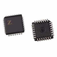
Z86E3116VSG Zilog, Z86E3116VSG Datasheet - Page 43

Z86E3116VSG
Manufacturer Part Number
Z86E3116VSG
Description
IC MICROCONTROLLER 2K 28-PLCC
Manufacturer
Zilog
Series
Z8®r
Datasheet
1.Z86E4001ZDV.pdf
(64 pages)
Specifications of Z86E3116VSG
Core Processor
Z8
Core Size
8-Bit
Speed
16MHz
Peripherals
POR, WDT
Number Of I /o
24
Program Memory Size
2KB (2K x 8)
Program Memory Type
OTP
Ram Size
125 x 8
Voltage - Supply (vcc/vdd)
3.5 V ~ 5.5 V
Oscillator Type
Internal
Operating Temperature
0°C ~ 70°C
Package / Case
28-PLCC
Processor Series
Z86E3xx
Core
Z8
Data Bus Width
8 bit
Data Ram Size
125 B
Maximum Clock Frequency
16 MHz
Number Of Programmable I/os
24
Number Of Timers
2
Operating Supply Voltage
3.5 V to 5.5 V
Maximum Operating Temperature
+ 70 C
Mounting Style
SMD/SMT
Minimum Operating Temperature
0 C
Lead Free Status / RoHS Status
Lead free / RoHS Compliant
Eeprom Size
-
Data Converters
-
Connectivity
-
Lead Free Status / Rohs Status
Details
Available stocks
Company
Part Number
Manufacturer
Quantity
Price
Zilog
SCLK/TCLK Divide-by-16 Select (D0). This bit of the
SMR controls a divide-by-16 prescaler of SCLK/TCLK.
The purpose of this control is to selectively reduce device
power consumption during normal processor execution
(SCLK control) and/or HALT mode (where TCLK sources
counter/timers and interrupt logic).
External Clock Divide-by-Two (D1). This bit can elimi-
nate the oscillator divide-by-two circuitry. When this bit is
0, the System Clock (SCLK) and Timer Clock (TCLK) are
equal to the external clock frequency divided by two. The
SCLK/TCLK is equal to the external clock frequency when
this bit is set (D1=1). Using this bit together with D7 of
DS97Z8X0502
SMR D4 D3 D2
Stop-Mode Recovery Edge
Select (SMR)
P33 From Pads
Digital/Analog Mode
Select (P3M)
0
VDD
0
P30
P31
P32
0
SMR
D4 D3 D2
0
0
0
0
1
1
P33
1
0
1
SMR
D4 D3 D2
1
0
Figure 32. Stop-Mode Recovery Source
P27
0
SMR2 D1 D0
SMR
0
P R E L I M I N A R Y
VDD
D4 D3 D2
1
0
0
P20
P23
1
P20
P23
PCON further helps lower EMI (i.e., D7 (PCON) = 0, D1
(SMR) = 1). The default setting is zero.
STOP-Mode Recovery Source (D2, D3, and D4). These
three bits of the SMR register specify the wake up source
of the STOP-Mode Recovery (Figure 32). Table 12 shows
the SMR source selected with the setting of D2 to D4.
P33–P31 cannot be used to wake up from STOP mode
when programmed as analog inputs. When the STOP-
Mode Recovery sources are selected in this register then
SMR2 register bits D0, D1 must be set to zero.
Note: If the Port2 pin is configured as an output, this output
level will be read by the SMR circuitry.
SMR
SMR2
D4 D3 D2
1
D1 D0
0
1
P20
P27
1
0
P20
P27
Z8 4K OTP Microcontroller
SMR
MUX
SMR2
D4 D3 D2
1
1
D1 D0
1
1
T o P33 Data
Latch and IRQ1
Z86E30/E31/E40
0
T o POR
RESET
43
1


