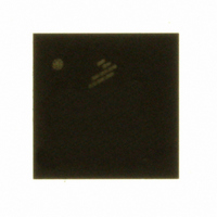
MC9S08QG84CFFE Freescale Semiconductor, MC9S08QG84CFFE Datasheet - Page 147

MC9S08QG84CFFE
Manufacturer Part Number
MC9S08QG84CFFE
Description
IC MCU 8BIT 8K FLASH 16-QFN
Manufacturer
Freescale Semiconductor
Series
HCS08r
Datasheet
1.MC9S08QG8CDTER.pdf
(314 pages)
Specifications of MC9S08QG84CFFE
Core Processor
HCS08
Core Size
8-Bit
Speed
20MHz
Connectivity
I²C, SCI, SPI
Peripherals
LVD, POR, PWM, WDT
Number Of I /o
12
Program Memory Size
8KB (8K x 8)
Program Memory Type
FLASH
Ram Size
512 x 8
Voltage - Supply (vcc/vdd)
1.8 V ~ 3.6 V
Data Converters
A/D 8x10b
Oscillator Type
Internal
Operating Temperature
-40°C ~ 85°C
Package / Case
16-QFN
Data Bus Width
8 bit
Data Ram Size
512 B
Interface Type
I2C, SCI, SPI
Maximum Clock Frequency
20 MHz
Number Of Programmable I/os
12
Number Of Timers
1
Maximum Operating Temperature
+ 85 C
Mounting Style
SMD/SMT
Minimum Operating Temperature
- 40 C
On-chip Adc
10 bit, 8 Channel
For Use With
DEMO9S08QG8E - BOARD DEMO FOR MC9S08QG8
Lead Free Status / RoHS Status
Lead free / RoHS Compliant
Eeprom Size
-
Lead Free Status / Rohs Status
Details
- Current page: 147 of 314
- Download datasheet (6Mb)
10.1.3
Key features of the ICS module are:
10.1.4
The ICS features the following modes of operation: FEI, FEE, FBI, FBILP, FBE, FBELP, and stop.
10.1.4.1
In FLL engaged internal mode, which is the default mode, the ICS supplies a clock derived from the FLL
which is controlled by the internal reference clock. The BDC clock is supplied from the FLL.
10.1.4.2
In FLL engaged external mode, the ICS supplies a clock derived from the FLL which is controlled by an
external reference clock. The BDC clock is supplied from the FLL.
10.1.4.3
In FLL bypassed internal mode, the FLL is enabled and controlled by the internal reference clock, but is
bypassed. The ICS supplies a clock derived from the internal reference clock. The BDC clock is supplied
from the FLL.
10.1.4.4
In FLL bypassed internal low power mode, the FLL is disabled and bypassed, and the ICS supplies a clock
derived from the internal reference clock. The BDC clock is not available.
Freescale Semiconductor
•
•
•
•
•
•
•
Frequency-locked loop (FLL) is trimmable for accuracy
— 0.2% resolution using internal 32 kHz reference
— 2% deviation over voltage and temperature using internal 32 kHz reference
External reference clock up to 5 MHz can be used to control the FLL
— 3 bit select for reference divider is provided
Internal reference clock has 9 trim bits available
Internal or external reference clock can be selected as the clock source for the MCU
Whichever clock is selected as the source can be divided down
— 2 bit select for clock divider is provided
Control signals for a low power oscillator as the external reference clock are provided
— HGO, RANGE, EREFS, ERCLKEN, EREFSTEN
FLL engaged internal mode is automatically selected out of reset
– Allowable dividers are: 1, 2, 4, 8
– BDC clock is provided as a constant divide by 2 of the DCO output
Features
Modes of Operation
FLL Engaged Interna
FLL Engaged External
FLL Bypassed Interna
FLL Bypassed Interna
MC9S08QG8 and MC9S08QG4 Data Sheet, Rev. 5
l (FEI)
l (FBI)
l Low Power (FBILP)
(FEE)
Internal Clock Source (S08ICSV1)
145
Related parts for MC9S08QG84CFFE
Image
Part Number
Description
Manufacturer
Datasheet
Request
R
Part Number:
Description:
Hcs08 Microcontrollers
Manufacturer:
Freescale Semiconductor, Inc
Datasheet:
Part Number:
Description:
Manufacturer:
Freescale Semiconductor, Inc
Datasheet:
Part Number:
Description:
Manufacturer:
Freescale Semiconductor, Inc
Datasheet:
Part Number:
Description:
Manufacturer:
Freescale Semiconductor, Inc
Datasheet:
Part Number:
Description:
Manufacturer:
Freescale Semiconductor, Inc
Datasheet:
Part Number:
Description:
Manufacturer:
Freescale Semiconductor, Inc
Datasheet:
Part Number:
Description:
Manufacturer:
Freescale Semiconductor, Inc
Datasheet:
Part Number:
Description:
Manufacturer:
Freescale Semiconductor, Inc
Datasheet:
Part Number:
Description:
Manufacturer:
Freescale Semiconductor, Inc
Datasheet:
Part Number:
Description:
Manufacturer:
Freescale Semiconductor, Inc
Datasheet:
Part Number:
Description:
Manufacturer:
Freescale Semiconductor, Inc
Datasheet:
Part Number:
Description:
Manufacturer:
Freescale Semiconductor, Inc
Datasheet:
Part Number:
Description:
Manufacturer:
Freescale Semiconductor, Inc
Datasheet:
Part Number:
Description:
Manufacturer:
Freescale Semiconductor, Inc
Datasheet:
Part Number:
Description:
Manufacturer:
Freescale Semiconductor, Inc
Datasheet:


