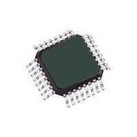
MC9S08JM8CLC Freescale Semiconductor, MC9S08JM8CLC Datasheet - Page 242

MC9S08JM8CLC
Manufacturer Part Number
MC9S08JM8CLC
Description
MCU 8BIT 8K FLASH 32-LQFP
Manufacturer
Freescale Semiconductor
Series
HCS08r
Datasheet
1.DEMO9S08JM16.pdf
(386 pages)
Specifications of MC9S08JM8CLC
Core Processor
HCS08
Core Size
8-Bit
Speed
48MHz
Connectivity
I²C, LIN, SCI, SPI, USB
Peripherals
LVD, POR, PWM, WDT
Number Of I /o
21
Program Memory Size
8KB (8K x 8)
Program Memory Type
FLASH
Ram Size
1K x 8
Voltage - Supply (vcc/vdd)
2.7 V ~ 5.5 V
Data Converters
A/D 4x12b
Oscillator Type
External
Operating Temperature
-40°C ~ 85°C
Package / Case
32-LQFP
Processor Series
S08JM
Core
HCS08
Data Bus Width
8 bit
Data Ram Size
1 KB
Interface Type
I2C, SPI
Maximum Clock Frequency
48 MHz
Number Of Programmable I/os
37
Number Of Timers
2
Operating Supply Voltage
2.7 V to 5.5 V
Maximum Operating Temperature
+ 85 C
Mounting Style
SMD/SMT
3rd Party Development Tools
EWS08
Development Tools By Supplier
DEMOJM, DEMOJMSKT, DEMOFLEXISJMSD, DEMO9S08JM16
Minimum Operating Temperature
- 40 C
On-chip Adc
12 bit, 4 Channel
Controller Family/series
HCS08
No. Of I/o's
21
Ram Memory Size
1KB
Cpu Speed
48MHz
No. Of Timers
2
Digital Ic Case Style
LQFP
Rohs Compliant
Yes
Lead Free Status / RoHS Status
Lead free / RoHS Compliant
Eeprom Size
-
Lead Free Status / Rohs Status
Lead free / RoHS Compliant
- Current page: 242 of 386
- Download datasheet (8Mb)
Serial Peripheral Interface (S08SPI16V1)
15.1.2
The SPI includes these distinctive features:
15.1.3
The SPI functions in three modes, run, wait, and stop.
The SPI is completely disabled in all other stop modes. When the CPU wakes from these stop modes, all
SPI register content will be reset.
This is a high level description only, detailed descriptions of operating modes are contained in section
Section 15.4.9, “Low Power Mode
15.1.4
This section includes block diagrams showing SPI system connections, the internal organization of the SPI
module, and the SPI clock dividers that control the master mode bit rate.
242
•
•
•
•
•
•
•
•
•
•
•
•
•
•
Master mode or slave mode operation
Full-duplex or single-wire bidirectional mode
Programmable transmit bit rate
Double-buffered transmit and receive data register
Serial clock phase and polarity options
Slave select output
Mode fault error flag with CPU interrupt capability
Control of SPI operation during wait mode
Selectable MSB-first or LSB-first shifting
Programmable 8- or 16-bit data transmission length
Receive data buffer hardware match feature
Run Mode
This is the basic mode of operation.
Wait Mode
SPI operation in wait mode is a configurable low power mode, controlled by the SPISWAI bit
located in the SPIxC2 register. In wait mode, if the SPISWAI bit is clear, the SPI operates like in
Run Mode. If the SPISWAI bit is set, the SPI goes into a power conservative state, with the SPI
clock generation turned off. If the SPI is configured as a master, any transmission in progress stops,
but is resumed after CPU goes into Run Mode. If the SPI is configured as a slave, reception and
transmission of a byte continues, so that the slave stays synchronized to the master.
Stop Mode
The SPI is inactive in stop3 mode for reduced power consumption. If the SPI is configured as a
master, any transmission in progress stops, but is resumed after the CPU goes into Run Mode. If
the SPI is configured as a slave, reception and transmission of a data continues, so that the slave
stays synchronized to the master.
Features
Modes of Operation
Block Diagrams
MC9S08JM16 Series Data Sheet, Rev. 2
Options.”
Freescale Semiconductor
Related parts for MC9S08JM8CLC
Image
Part Number
Description
Manufacturer
Datasheet
Request
R
Part Number:
Description:
Manufacturer:
Freescale Semiconductor, Inc
Datasheet:
Part Number:
Description:
Manufacturer:
Freescale Semiconductor, Inc
Datasheet:
Part Number:
Description:
Manufacturer:
Freescale Semiconductor, Inc
Datasheet:
Part Number:
Description:
Manufacturer:
Freescale Semiconductor, Inc
Datasheet:
Part Number:
Description:
Manufacturer:
Freescale Semiconductor, Inc
Datasheet:
Part Number:
Description:
Manufacturer:
Freescale Semiconductor, Inc
Datasheet:
Part Number:
Description:
Manufacturer:
Freescale Semiconductor, Inc
Datasheet:
Part Number:
Description:
Manufacturer:
Freescale Semiconductor, Inc
Datasheet:
Part Number:
Description:
Manufacturer:
Freescale Semiconductor, Inc
Datasheet:
Part Number:
Description:
Manufacturer:
Freescale Semiconductor, Inc
Datasheet:
Part Number:
Description:
Manufacturer:
Freescale Semiconductor, Inc
Datasheet:
Part Number:
Description:
Manufacturer:
Freescale Semiconductor, Inc
Datasheet:
Part Number:
Description:
Manufacturer:
Freescale Semiconductor, Inc
Datasheet:
Part Number:
Description:
Manufacturer:
Freescale Semiconductor, Inc
Datasheet:
Part Number:
Description:
Manufacturer:
Freescale Semiconductor, Inc
Datasheet:


