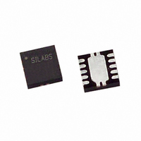
C8051F301-GMR Silicon Laboratories Inc, C8051F301-GMR Datasheet - Page 104

C8051F301-GMR
Manufacturer Part Number
C8051F301-GMR
Description
IC 8051 MCU 8K FLASH 11QFN
Manufacturer
Silicon Laboratories Inc
Series
C8051F30xr
Specifications of C8051F301-GMR
Core Processor
8051
Core Size
8-Bit
Speed
25MHz
Connectivity
SMBus (2-Wire/I²C), UART/USART
Peripherals
POR, PWM, WDT
Number Of I /o
8
Program Memory Size
8KB (8K x 8)
Program Memory Type
FLASH
Ram Size
256 x 8
Voltage - Supply (vcc/vdd)
2.7 V ~ 3.6 V
Oscillator Type
Internal
Operating Temperature
-40°C ~ 85°C
Package / Case
11-VQFN
Package
11QFN EP
Device Core
8051
Family Name
C8051F30x
Maximum Speed
25 MHz
Operating Supply Voltage
3.3 V
Data Bus Width
8 Bit
Number Of Programmable I/os
8
Interface Type
I2C/SMBus/UART
Number Of Timers
3
For Use With
336-1444 - ADAPTER PROGRAM TOOLSTICK F300336-1319 - REFERENCE DESIGN STEPPER MOTOR
Lead Free Status / RoHS Status
Lead free / RoHS Compliant
Eeprom Size
-
Data Converters
-
Available stocks
Company
Part Number
Manufacturer
Quantity
Price
C8051F300/1/2/3/4/5
12.1. Priority Crossbar Decoder
The Priority Crossbar Decoder (Figure 12.3) assigns a priority to each I/O function, starting at the top with
UART0. When a digital resource is selected, the least significant unassigned Port pin is assigned to that
resource (excluding UART0, which is always at pins 4 and 5). If a Port pin is assigned, the Crossbar skips
that pin when assigning the next selected resource. Additionally, the Crossbar will skip Port pins whose
associated bits in the XBR0 register are set. The XBR0 register allows software to skip Port pins that are to
be used for analog input or GPIO.
Important Note on Crossbar Configuration: If a Port pin is claimed by a peripheral without use of the
Crossbar, its corresponding XBR0 bit should be set. This applies to P0.0 if VREF is enabled, P0.3 and/or
P0.2 if the external oscillator circuit is enabled, P0.6 if the ADC is configured to use the external conversion
start signal (CNVSTR), and any selected ADC or Comparator inputs. The Crossbar skips selected pins as
if they were already assigned, and moves to the next unassigned pin. Figure 12.3 shows the Crossbar
Decoder priority with no Port pins skipped (XBR0 = 0x00); Figure 12.4 shows the Crossbar Decoder prior-
ity with pins 6 and 2 skipped (XBR0 = 0x44).
104
Figure 12.3. Crossbar Priority Decoder with XBR0 = 0x00
SF Signals
PIN I/O
TX0
RX0
SDA
SCL
CP0
CP0A
SYSCLK
CEX0
CEX1
CEX2
ECI
T0
T1
SF Signals
VREF
Port pin potentially available to peripheral
Special Function Signals are not assigned by the crossbar.
When these signals are enabled, the CrossBar must be
manually configured to skip their corresponding port pins.
Note: x1 refers to the XTAL1 signal; x2 refers to the XTAL2
signal.
0
0
1
0
x1
2
0
XBR0[0:7]
x2
3
0
Rev. 2.9
P0
4
0
5
0
CNVSTR
6
0
7
0


