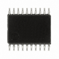
R5F211B1SP#U0 Renesas Electronics America, R5F211B1SP#U0 Datasheet - Page 28

R5F211B1SP#U0
Manufacturer Part Number
R5F211B1SP#U0
Description
IC R8C MCU FLASH 4K 20SSOP
Manufacturer
Renesas Electronics America
Series
M16C™ M16C/R8C/Tiny/1Br
Datasheets
1.R5F211A2SPU0.pdf
(51 pages)
2.R5F211A2SPU0.pdf
(300 pages)
3.R5F211A2SPU0.pdf
(341 pages)
Specifications of R5F211B1SP#U0
Core Processor
R8C
Core Size
16-Bit
Speed
20MHz
Connectivity
I²C, SIO, SSU, UART/USART
Peripherals
LED, POR, Voltage Detect, WDT
Number Of I /o
13
Program Memory Size
4KB (4K x 8)
Program Memory Type
FLASH
Ram Size
384 x 8
Voltage - Supply (vcc/vdd)
2.7 V ~ 5.5 V
Data Converters
A/D 4x10b
Oscillator Type
Internal
Operating Temperature
-20°C ~ 85°C
Package / Case
20-SSOP
For Use With
R0K5211B4S001BE - KIT STARTER FOR R8C/18191A1BR0K5211B4S000BE - KIT DEV EVALUATION R8C/1BR0E521174CPE10 - EMULATOR COMPACT R8C/18/19/1
Lead Free Status / RoHS Status
Lead free / RoHS Compliant
Eeprom Size
-
Available stocks
Company
Part Number
Manufacturer
Quantity
Price
- Current page: 28 of 300
- Download datasheet (2Mb)
Rev.2.00 Oct 17, 2005
REJ09B0001-0200
1.5 Register Banks
Chapter 1 Overview
The R8C/Tiny has two register banks, each comprising data registers (R0, R1, R2, and R3), address regis-
ters (A0 and A1), and a frame base register (FB). These two register banks are switched by the register
bank select flag (B flag) in the flag register (FLG).
Figure 1.5.1 shows the configuration of the register banks.
Figure 1.5.1 Configuration of Register Banks
Register bank 0 (B flag = 0)
R0
R1
R2
R3
A0
A1
FB
page 8 of 263
b15
H
H
b8b7
L
L
b0
R0
R1
R2
R3
A0
A1
FB
Register bank 1 (B flag = 1)
b15
H
H
b8b7
1.5 Register Banks
L
L
b0
Related parts for R5F211B1SP#U0
Image
Part Number
Description
Manufacturer
Datasheet
Request
R

Part Number:
Description:
KIT STARTER FOR M16C/29
Manufacturer:
Renesas Electronics America
Datasheet:

Part Number:
Description:
KIT STARTER FOR R8C/2D
Manufacturer:
Renesas Electronics America
Datasheet:

Part Number:
Description:
R0K33062P STARTER KIT
Manufacturer:
Renesas Electronics America
Datasheet:

Part Number:
Description:
KIT STARTER FOR R8C/23 E8A
Manufacturer:
Renesas Electronics America
Datasheet:

Part Number:
Description:
KIT STARTER FOR R8C/25
Manufacturer:
Renesas Electronics America
Datasheet:

Part Number:
Description:
KIT STARTER H8S2456 SHARPE DSPLY
Manufacturer:
Renesas Electronics America
Datasheet:

Part Number:
Description:
KIT STARTER FOR R8C38C
Manufacturer:
Renesas Electronics America
Datasheet:

Part Number:
Description:
KIT STARTER FOR R8C35C
Manufacturer:
Renesas Electronics America
Datasheet:

Part Number:
Description:
KIT STARTER FOR R8CL3AC+LCD APPS
Manufacturer:
Renesas Electronics America
Datasheet:

Part Number:
Description:
KIT STARTER FOR RX610
Manufacturer:
Renesas Electronics America
Datasheet:

Part Number:
Description:
KIT STARTER FOR R32C/118
Manufacturer:
Renesas Electronics America
Datasheet:

Part Number:
Description:
KIT DEV RSK-R8C/26-29
Manufacturer:
Renesas Electronics America
Datasheet:

Part Number:
Description:
KIT STARTER FOR SH7124
Manufacturer:
Renesas Electronics America
Datasheet:

Part Number:
Description:
KIT STARTER FOR H8SX/1622
Manufacturer:
Renesas Electronics America
Datasheet:

Part Number:
Description:
KIT DEV FOR SH7203
Manufacturer:
Renesas Electronics America
Datasheet:


