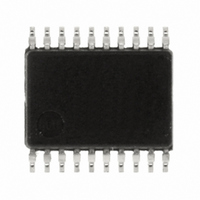
R5F211B1SP#U0 Renesas Electronics America, R5F211B1SP#U0 Datasheet - Page 144

R5F211B1SP#U0
Manufacturer Part Number
R5F211B1SP#U0
Description
IC R8C MCU FLASH 4K 20SSOP
Manufacturer
Renesas Electronics America
Series
M16C™ M16C/R8C/Tiny/1Br
Datasheets
1.R5F211A2SPU0.pdf
(51 pages)
2.R5F211A2SPU0.pdf
(300 pages)
3.R5F211A2SPU0.pdf
(341 pages)
Specifications of R5F211B1SP#U0
Core Processor
R8C
Core Size
16-Bit
Speed
20MHz
Connectivity
I²C, SIO, SSU, UART/USART
Peripherals
LED, POR, Voltage Detect, WDT
Number Of I /o
13
Program Memory Size
4KB (4K x 8)
Program Memory Type
FLASH
Ram Size
384 x 8
Voltage - Supply (vcc/vdd)
2.7 V ~ 5.5 V
Data Converters
A/D 4x10b
Oscillator Type
Internal
Operating Temperature
-20°C ~ 85°C
Package / Case
20-SSOP
For Use With
R0K5211B4S001BE - KIT STARTER FOR R8C/18191A1BR0K5211B4S000BE - KIT DEV EVALUATION R8C/1BR0E521174CPE10 - EMULATOR COMPACT R8C/18/19/1
Lead Free Status / RoHS Status
Lead free / RoHS Compliant
Eeprom Size
-
Available stocks
Company
Part Number
Manufacturer
Quantity
Price
- Current page: 144 of 341
- Download datasheet (4Mb)
R8C/1A Group, R8C/1B Group
Rev.1.30
REJ09B0252-0130
Figure 14.14
Timer Z Output Control Register
Timer Z Waveform Output Control Register
b7 b6 b5 b4
NOTES :
b7 b6 b5 b4
NOTES :
1.
2.
3. When executing an instruction w hich changes this register w hen the TZOS bit is set to 1 (during count), the TZOS
1.
2.
This bit is set to 0 w hen the output of a one-shot w aveform is completed. If the TZS bit in the TZMR register w as set
to 0 (count stops) to stop the w aveform output during one-shot w aveform output, set the TZOS bit to 0.
This bit is enabled only w hen operating in programmable w aveform generation mode.
bit is automatically set to 0 (one-shot stop) if the count is completed w hile the instruction is being executed. If this
causes problems, execute an instruction w hich changes the contents of this register w hen the TZOS bit is set to 0
(one-shot stop).
The INOSEG bit is enabled only w hen the INT0PL bit in the INTEN register is set to 0 (one edge).
Set the INOSTG bit to 1 after setting the INT0EN bit in the INTEN register and the INOSEG bit in the PUM register.
Dec 08, 2006
0
b3 b2 b1 b0
b3 b2
0
0
Registers TZOC and PUM
0
b1 b0
0
0
Bit Symbol
Bit Symbol
TZOCNT
(b7-b3)
INOSTG
INOSEG
Symbol
(b4-b0)
Symbol
TZOPL
TZOC
TZOS
(b1)
PUM
Page 126 of 315
—
—
—
Timer Z one-shot start bit
Reserved bit
Timer Z programmable w aveform
generation output sw itch bit
Nothing is assigned. If necessary, set to 0.
When read, the content is 0.
Reserved bits
Timer Z output level latch
_____
INT0
bit (timer Z)
_____
INT0
select bit (timer Z)
(3)
pin one-shot trigger control
pin one-shot trigger polarity
(2)
Address
Bit Name
Address
Bit Name
008Ah
0084h
(1)
(1)
(2)
0 : One-shot stops.
1 : One-shot starts.
Set to 0.
0 : Outputs programmable w aveform.
1 : Outputs value in P1_3 port register.
Set to 0.
Function varies depending on operating
mode.
0 : INT0
1 : INT0
0 : Falling edge trigger
1 : Rising edge trigger
_____
_____
pin one-shot trigger disabled
pin one-shot trigger enabled
After Reset
After Reset
Function
Function
00h
00h
14. Timers
RW
RW
RW
RW
RW
RW
RW
RW
RW
—
Related parts for R5F211B1SP#U0
Image
Part Number
Description
Manufacturer
Datasheet
Request
R

Part Number:
Description:
KIT STARTER FOR M16C/29
Manufacturer:
Renesas Electronics America
Datasheet:

Part Number:
Description:
KIT STARTER FOR R8C/2D
Manufacturer:
Renesas Electronics America
Datasheet:

Part Number:
Description:
R0K33062P STARTER KIT
Manufacturer:
Renesas Electronics America
Datasheet:

Part Number:
Description:
KIT STARTER FOR R8C/23 E8A
Manufacturer:
Renesas Electronics America
Datasheet:

Part Number:
Description:
KIT STARTER FOR R8C/25
Manufacturer:
Renesas Electronics America
Datasheet:

Part Number:
Description:
KIT STARTER H8S2456 SHARPE DSPLY
Manufacturer:
Renesas Electronics America
Datasheet:

Part Number:
Description:
KIT STARTER FOR R8C38C
Manufacturer:
Renesas Electronics America
Datasheet:

Part Number:
Description:
KIT STARTER FOR R8C35C
Manufacturer:
Renesas Electronics America
Datasheet:

Part Number:
Description:
KIT STARTER FOR R8CL3AC+LCD APPS
Manufacturer:
Renesas Electronics America
Datasheet:

Part Number:
Description:
KIT STARTER FOR RX610
Manufacturer:
Renesas Electronics America
Datasheet:

Part Number:
Description:
KIT STARTER FOR R32C/118
Manufacturer:
Renesas Electronics America
Datasheet:

Part Number:
Description:
KIT DEV RSK-R8C/26-29
Manufacturer:
Renesas Electronics America
Datasheet:

Part Number:
Description:
KIT STARTER FOR SH7124
Manufacturer:
Renesas Electronics America
Datasheet:

Part Number:
Description:
KIT STARTER FOR H8SX/1622
Manufacturer:
Renesas Electronics America
Datasheet:

Part Number:
Description:
KIT DEV FOR SH7203
Manufacturer:
Renesas Electronics America
Datasheet:


