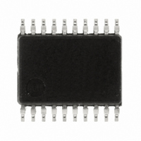
R5F211B1SP#U0 Renesas Electronics America, R5F211B1SP#U0 Datasheet - Page 4

R5F211B1SP#U0
Manufacturer Part Number
R5F211B1SP#U0
Description
IC R8C MCU FLASH 4K 20SSOP
Manufacturer
Renesas Electronics America
Series
M16C™ M16C/R8C/Tiny/1Br
Datasheets
1.R5F211A2SPU0.pdf
(51 pages)
2.R5F211A2SPU0.pdf
(300 pages)
3.R5F211A2SPU0.pdf
(341 pages)
Specifications of R5F211B1SP#U0
Core Processor
R8C
Core Size
16-Bit
Speed
20MHz
Connectivity
I²C, SIO, SSU, UART/USART
Peripherals
LED, POR, Voltage Detect, WDT
Number Of I /o
13
Program Memory Size
4KB (4K x 8)
Program Memory Type
FLASH
Ram Size
384 x 8
Voltage - Supply (vcc/vdd)
2.7 V ~ 5.5 V
Data Converters
A/D 4x10b
Oscillator Type
Internal
Operating Temperature
-20°C ~ 85°C
Package / Case
20-SSOP
For Use With
R0K5211B4S001BE - KIT STARTER FOR R8C/18191A1BR0K5211B4S000BE - KIT DEV EVALUATION R8C/1BR0E521174CPE10 - EMULATOR COMPACT R8C/18/19/1
Lead Free Status / RoHS Status
Lead free / RoHS Compliant
Eeprom Size
-
Available stocks
Company
Part Number
Manufacturer
Quantity
Price
R8C/1A Group, R8C/1B Group
Rev.1.40
REJ03B0144-0140
1.2
Table 1.1
NOTE:
CPU
Peripheral
Functions
Electric
Characteristics
Flash Memory
Operating Ambient Temperature
Package
Table 1.1 outlines the Functions and Specifications for R8C/1A Group and Table 1.2 outlines the
Functions and Specifications for R8C/1B Group.
1. I
2. Please contact Renesas Technology sales offices for the Y version.
2
Performance Overview
C bus is a trademark of Koninklijke Philips Electronics N. V.
Dec 08, 2006
Functions and Specifications for R8C/1A Group
Number of fundamental
instructions
Minimum instruction execution
time
Operating mode
Address space
Memory capacity
Ports
LED drive ports
Timers
Serial interfaces
Clock synchronous serial interface 1 channel
A/D converter
Watchdog timer
Interrupts
Clock generation circuits
Oscillation stop detection function
Voltage detection circuit
Power-on reset circuit
Supply voltage
Current consumption
Programming and erasure voltage VCC = 2.7 to 5.5 V
Programming and erasure
endurance
Item
Page 2 of 45
89 instructions
50 ns (f(XIN) = 20 MHz, VCC = 3.0 to 5.5 V)
100 ns (f(XIN) = 10 MHz, VCC = 2.7 to 5.5 V)
Single-chip
1 Mbyte
See Table 1.3 Product Information for R8C/1A Group
I/O ports: 13 pins (including LED drive port)
Input port: 3 pins
I/O ports: 4 pins
Timer X: 8 bits × 1 channel, timer Z: 8 bits × 1 channel
(Each timer equipped with 8-bit prescaler)
Timer C: 16 bits × 1 channel
(Input capture and output compare circuits)
1 channel
1 channel
10-bit A/D converter: 1 circuit, 4 channels
15 bits × 1 channel (with prescaler)
Internal: 11 sources, External: 4 sources, Software: 4 sources,
Priority levels: 7 levels
2 circuits
Main clock oscillation stop detection function
On-chip
On-chip
VCC = 3.0 to 5.5 V (f(XIN) = 20 MHz)
VCC = 2.7 to 5.5 V (f(XIN) = 10 MHz)
Typ. 9 mA (VCC = 5.0 V, f(XIN) = 20 MHz, A/D converter stopped)
Typ. 5 mA (VCC = 3.0 V, f(XIN) = 10 MHz, A/D converter stopped)
Typ. 35 µA (VCC = 3.0 V, wait mode, peripheral clock off)
Typ. 0.7 µA (VCC = 3.0 V, stop mode)
100 times
-20 to 85°C
-40 to 85°C (D version)
-20 to 105°C (Y version)
20-pin molded-plastic LSSOP
20-pin molded-plastic SDIP
28-pin molded-plastic HWQFN
• Main clock oscillation circuit (with on-chip feedback resistor)
• On-chip oscillator (high speed, low speed)
Reset start selectable, count source protection mode
High-speed on-chip oscillator has a frequency adjustment
function
Clock synchronous serial I/O, UART
UART
I
Clock synchronous serial I/O with chip select (SSU)
2
C bus Interface
(1)
Specification
(2)
1. Overview


