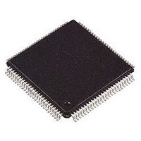
MC908GR32ACFAER Freescale Semiconductor, MC908GR32ACFAER Datasheet - Page 67

MC908GR32ACFAER
Manufacturer Part Number
MC908GR32ACFAER
Description
IC MCU 32K FLASH 8MHZ 48-LQFP
Manufacturer
Freescale Semiconductor
Series
HC08r
Datasheet
1.MC908GR32ACFJE.pdf
(314 pages)
Specifications of MC908GR32ACFAER
Core Processor
HC08
Core Size
8-Bit
Speed
8MHz
Connectivity
SCI, SPI
Peripherals
LVD, POR, PWM
Number Of I /o
37
Program Memory Size
32KB (32K x 8)
Program Memory Type
FLASH
Ram Size
1.5K x 8
Voltage - Supply (vcc/vdd)
3 V ~ 5.5 V
Data Converters
A/D 24x10b
Oscillator Type
Internal
Operating Temperature
-40°C ~ 85°C
Package / Case
48-LQFP
Controller Family/series
HC08
No. Of I/o's
37
Ram Memory Size
1.5KB
Cpu Speed
8MHz
No. Of Timers
2
Embedded Interface Type
SCI, SPI
Rohs Compliant
Yes
Processor Series
HC08GR
Core
HC08
Data Bus Width
8 bit
Data Ram Size
1.5 KB
Interface Type
ESCI, SPI
Maximum Clock Frequency
8 MHz
Number Of Programmable I/os
53
Number Of Timers
8
Maximum Operating Temperature
+ 85 C
Mounting Style
SMD/SMT
Development Tools By Supplier
FSICEBASE, DEMO908GZ60E, M68CBL05CE, M68EML08GPGTE
Minimum Operating Temperature
- 40 C
On-chip Adc
10 bit, 24 Channel
Lead Free Status / RoHS Status
Lead free / RoHS Compliant
Eeprom Size
-
Lead Free Status / Rohs Status
Details
Available stocks
Company
Part Number
Manufacturer
Quantity
Price
Company:
Part Number:
MC908GR32ACFAER
Manufacturer:
Freescale Semiconductor
Quantity:
10 000
- Current page: 67 of 314
- Download datasheet (5Mb)
3.8.2 ADC Data Register High and Data Register Low
3.8.2.1 Left Justified Mode
In left justified mode, the ADRH register holds the eight MSBs of the
10-bit result. The ADRL register holds the two LSBs of the 10-bit result. All other bits read as 0. ADRH
and ADRL are updated each time an ADC single channel conversion completes. Reading ADRH latches
the contents of ADRL until ADRL is read. All subsequent results will be lost until the ADRH and ADRL
reads are completed.
Freescale Semiconductor
Address:
Address:
1. If any unused channels are selected, the resulting ADC conversion will be unknown or re-
ADCH4
Reset:
Reset:
Read:
Read:
Write:
Write:
served.
MC68HC908GR60A • MC68HC908GR48A • MC68HC908GR32A Data Sheet, Rev. 5
1
1
1
1
1
1
1
1
1
↓
1
1
1
1
Figure 3-5. ADC Data Register High (ADRH) and Low (ADRL)
$003D
$003E
Bit 7
AD9
AD1
ADCH3
Table 3-1. Mux Channel Select
↓
0
0
0
0
0
0
0
0
1
1
1
1
1
= Unimplemented
AD8
AD0
6
ADCH2
0
0
0
0
1
1
1
1
0
↓
1
1
1
1
AD7
5
0
ADCH1
Unaffected by reset
Unaffected by reset
AD6
↓
0
0
1
1
0
0
1
1
0
0
0
1
1
4
0
AD5
ADCH0
(1)
3
0
0
1
0
1
0
1
0
1
0
↓
0
1
0
1
(Continued)
AD4
2
0
ADC power off
Input Select
PTG0/AD16
PTG1/AD17
PTG2/AD18
PTG3/AD19
PTG4/AD20
PTG5/AD21
PTG6/AD22
PTG7/AD23
Unused
V
V
AD3
REFH
1
0
REFL
ADRH
ADRL
Bit 0
AD2
0
I/O Registers
67
Related parts for MC908GR32ACFAER
Image
Part Number
Description
Manufacturer
Datasheet
Request
R
Part Number:
Description:
Manufacturer:
Freescale Semiconductor, Inc
Datasheet:
Part Number:
Description:
Manufacturer:
Freescale Semiconductor, Inc
Datasheet:
Part Number:
Description:
Manufacturer:
Freescale Semiconductor, Inc
Datasheet:
Part Number:
Description:
Manufacturer:
Freescale Semiconductor, Inc
Datasheet:
Part Number:
Description:
Manufacturer:
Freescale Semiconductor, Inc
Datasheet:
Part Number:
Description:
Manufacturer:
Freescale Semiconductor, Inc
Datasheet:
Part Number:
Description:
Manufacturer:
Freescale Semiconductor, Inc
Datasheet:
Part Number:
Description:
Manufacturer:
Freescale Semiconductor, Inc
Datasheet:
Part Number:
Description:
Manufacturer:
Freescale Semiconductor, Inc
Datasheet:
Part Number:
Description:
Manufacturer:
Freescale Semiconductor, Inc
Datasheet:
Part Number:
Description:
Manufacturer:
Freescale Semiconductor, Inc
Datasheet:
Part Number:
Description:
Manufacturer:
Freescale Semiconductor, Inc
Datasheet:
Part Number:
Description:
Manufacturer:
Freescale Semiconductor, Inc
Datasheet:
Part Number:
Description:
Manufacturer:
Freescale Semiconductor, Inc
Datasheet:
Part Number:
Description:
Manufacturer:
Freescale Semiconductor, Inc
Datasheet:


