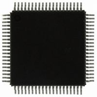
MC9S12C96CFUE Freescale Semiconductor, MC9S12C96CFUE Datasheet - Page 139

MC9S12C96CFUE
Manufacturer Part Number
MC9S12C96CFUE
Description
IC MCU 96K FLASH 4K RAM 80-QFP
Manufacturer
Freescale Semiconductor
Series
HCS12r
Specifications of MC9S12C96CFUE
Core Processor
HCS12
Core Size
16-Bit
Speed
25MHz
Connectivity
CAN, EBI/EMI, SCI, SPI
Peripherals
POR, PWM, WDT
Number Of I /o
60
Program Memory Size
96KB (96K x 8)
Program Memory Type
FLASH
Ram Size
4K x 8
Voltage - Supply (vcc/vdd)
2.35 V ~ 5.5 V
Data Converters
A/D 8x10b
Oscillator Type
Internal
Operating Temperature
-40°C ~ 85°C
Package / Case
80-QFP
Processor Series
S12C
Core
HCS12
Data Bus Width
16 bit
Data Ram Size
4 KB
Interface Type
CAN/SCI/SPI
Maximum Clock Frequency
25 MHz
Number Of Programmable I/os
60
Number Of Timers
8
Operating Supply Voltage
- 0.3 V to + 6.5 V
Maximum Operating Temperature
+ 85 C
Mounting Style
SMD/SMT
3rd Party Development Tools
EWHCS12
Development Tools By Supplier
M68EVB912C32EE
Minimum Operating Temperature
- 40 C
On-chip Adc
8-ch x 10-bit
Lead Free Status / RoHS Status
Lead free / RoHS Compliant
Eeprom Size
-
Lead Free Status / Rohs Status
Lead free / RoHS Compliant
Available stocks
Company
Part Number
Manufacturer
Quantity
Price
Company:
Part Number:
MC9S12C96CFUE
Manufacturer:
Freescale Semiconductor
Quantity:
10 000
Company:
Part Number:
MC9S12C96CFUER
Manufacturer:
Freescale Semiconductor
Quantity:
10 000
- Current page: 139 of 690
- Download datasheet (4Mb)
These register locations are not used (reserved). All unused registers and bits in this block return logic 0s
when read. Writes to these registers have no effect.
These registers are not in the on-chip map in special peripheral mode.
4.3.2.6
Read: Anytime when register is in the map
Write: Anytime when register is in the map
Port E is associated with external bus control signals and interrupt inputs. These include mode select
(MODB/IPIPE1, MODA/IPIPE0), E clock, size (LSTRB/TAGLO), read/write (R/W), IRQ, and XIRQ.
When not used for one of these specific functions, port E pins 7:2 can be used as general-purpose I/O and
pins 1:0 can be used as general-purpose input. The port E assignment register (PEAR) selects the function
of each pin and DDRE determines whether each pin is an input or output when it is configured to be
general-purpose I/O. DDRE also determines the source of data for a read of PORTE.
Some of these pins have software selectable pull resistors. IRQ and XIRQ can only be pulled up whereas
the polarity of the PE7, PE4, PE3, and PE2 pull resistors are determined by chip integration. Please refer
to the device overview chapter (Signal Property Summary) to determine the polarity of these resistors.
A single control bit enables the pull devices for all of these pins when they are configured as inputs.
This register is not in the on-chip map in special peripheral mode or in expanded modes when the EME
bit is set. Therefore, these accesses will be echoed externally.
Freescale Semiconductor
Module Base + 0x0008
Starting address location affected by INITRG register setting.
Pin Function
Alternate
Reset
W
R
Port E Data Register (PORTE)
NOACC
It is unwise to write PORTE and DDRE as a word access. If you are
changing port E pins from being inputs to outputs, the data may have extra
transitions during the write. It is best to initialize PORTE before enabling as
outputs.
Bit 7
0
7
= Unimplemented or Reserved
or CLKTO
or IPIPE1
MODB
6
0
6
Figure 4-10. Port E Data Register (PORTE)
MC9S12C-Family / MC9S12GC-Family
or IPIPE0
MODA
5
0
5
Rev 01.24
NOTE
ECLK
4
0
4
u = Unaffected by reset
or TAGLO
LSTRB
Chapter 4 Multiplexed External Bus Interface (MEBIV3)
3
3
0
R/W
2
2
0
Bit 1
IRQ
u
1
XIRQ
Bit 0
u
0
139
Related parts for MC9S12C96CFUE
Image
Part Number
Description
Manufacturer
Datasheet
Request
R
Part Number:
Description:
Manufacturer:
Freescale Semiconductor, Inc
Datasheet:
Part Number:
Description:
Manufacturer:
Freescale Semiconductor, Inc
Datasheet:
Part Number:
Description:
Manufacturer:
Freescale Semiconductor, Inc
Datasheet:
Part Number:
Description:
Manufacturer:
Freescale Semiconductor, Inc
Datasheet:
Part Number:
Description:
Manufacturer:
Freescale Semiconductor, Inc
Datasheet:
Part Number:
Description:
Manufacturer:
Freescale Semiconductor, Inc
Datasheet:
Part Number:
Description:
Manufacturer:
Freescale Semiconductor, Inc
Datasheet:
Part Number:
Description:
Manufacturer:
Freescale Semiconductor, Inc
Datasheet:
Part Number:
Description:
Manufacturer:
Freescale Semiconductor, Inc
Datasheet:
Part Number:
Description:
Manufacturer:
Freescale Semiconductor, Inc
Datasheet:
Part Number:
Description:
Manufacturer:
Freescale Semiconductor, Inc
Datasheet:
Part Number:
Description:
Manufacturer:
Freescale Semiconductor, Inc
Datasheet:
Part Number:
Description:
Manufacturer:
Freescale Semiconductor, Inc
Datasheet:
Part Number:
Description:
Manufacturer:
Freescale Semiconductor, Inc
Datasheet:
Part Number:
Description:
Manufacturer:
Freescale Semiconductor, Inc
Datasheet:


