DF2116VT20V Renesas Electronics America, DF2116VT20V Datasheet
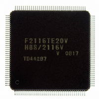
DF2116VT20V
Specifications of DF2116VT20V
DF2116VTE20V
Available stocks


Related parts for DF2116VT20V


DF2116VT20V Summary of contents
Page 1
To our customers, Old Company Name in Catalogs and Other Documents st On April 1 , 2010, NEC Electronics Corporation merged with Renesas Technology Corporation, and Renesas Electronics Corporation took over all the business of both companies. Therefore, although the ...
Page 2
All information included in this document is current as of the date this document is issued. Such information, however, is subject to change without any prior notice. Before purchasing or using any Renesas Electronics products listed herein, please confirm ...
Page 3
H8S/2116 Group 16 Hardware Manual Renesas 16-Bit Single-Chip Microcomputer H8S Family / H8S/2100 Series H8S/2116 R4F2116 Rev.1.00 2006.03 ...
Page 4
Rev. 1.00 Mar. 02, 2006 Page ...
Page 5
Keep safety first in your circuit designs! 1. Renesas Technology Corp. puts the maximum effort into making semiconductor products better and more reliable, but there is always the possibility that trouble may occur with them. Trouble with semiconductors may lead ...
Page 6
General Precautions on Handling of Product 1. Treatment of NC Pins Note: Do not connect anything to the NC pins. The NC (not connected) pins are either not connected to any of the internal circuitry or are used as test ...
Page 7
Configuration of This Manual This manual comprises the following items: 1. General Precautions on Handling of Product 2. Configuration of This Manual 3. Preface 4. Contents 5. Overview 6. Description of Functional Modules • CPU and System-Control Modules • On-Chip ...
Page 8
This H8S/2116 Group is a series of microcomputers (MCUs) made up of the H8S/2000 CPU with Renesas Technology's original architecture as its core, and the peripheral functions required to configure a system. The H8S/2000 CPU has an internal 32-bit configuration, ...
Page 9
In order to understand the details of the CPU's functions Read the H8S/2600 Series, H8S/2000 Series Programming Manual. • In order to understand the detailed function of a register whose name is known Read the index that is the ...
Page 10
Rev. 1.00 Mar. 02, 2006 Page viii of xl ...
Page 11
Section 1 Overview................................................................................................1 1.1 Overview............................................................................................................................... 1 1.2 Internal Block Diagram......................................................................................................... 3 1.3 Pin Description ..................................................................................................................... 4 1.3.1 Pin Arrangement ................................................................................................... 4 1.3.2 Pin Arrangement in Each Operating Mode........................................................... 6 1.3.3 Pin Functions ...................................................................................................... 11 Section 2 CPU......................................................................................................19 2.1 Features............................................................................................................................... 19 ...
Page 12
Immediate—#xx:8, #xx:16, or #xx:32................................................................ 49 2.7.7 Program-Counter Relative—@(d:8, PC) or @(d:16, PC) .................................. 49 2.7.8 Memory Indirect—@@aa:8 ............................................................................... 50 2.7.9 Effective Address Calculation ............................................................................ 51 2.8 Processing States ................................................................................................................ 53 2.9 Usage Notes ........................................................................................................................ 55 2.9.1 Note on TAS ...
Page 13
Break Address Registers (BARA to BARC)........................................... 81 5.3.4 IRQ Sense Control Registers (ISCR16H, ISCR16L, ISCRH, ISCRL)............... 82 5.3.5 IRQ Enable Registers (IER16, IER) ................................................................... 84 5.3.6 IRQ Status Registers (ISR16, ISR) ..................................................................... 85 5.3.7 Keyboard Matrix ...
Page 14
Port 1 Data Direction Register (P1DDR).......................................................... 126 7.1.2 Port 1 Data Register (P1DR)............................................................................. 126 7.1.3 Port 1 Pull-Up MOS Control Register (P1PCR)............................................... 127 7.1.4 Pin Functions .................................................................................................... 127 7.1.5 Port 1 Input Pull-Up MOS ................................................................................ 127 7.2 Port 2................................................................................................................................. ...
Page 15
Pin Functions .................................................................................................... 147 7.9 Port 9................................................................................................................................. 150 7.9.1 Port 9 Data Direction Register (P9DDR).......................................................... 150 7.9.2 Port 9 Data Register (P9DR)............................................................................. 151 7.9.3 Port 9 Pull-Up MOS Control Register (P9PCR)............................................... 151 7.9.4 Pin Functions .................................................................................................... 152 7.9.5 Input ...
Page 16
Port F ................................................................................................................................ 175 7.15.1 Port F Data Direction Register (PFDDR) ......................................................... 175 7.15.2 Port F Output Data Register (PFODR) ............................................................. 176 7.15.3 Port F Input Data Register (PFPIN).................................................................. 176 7.15.4 Pin Functions .................................................................................................... 177 7.15.5 Port F Nch-OD ...
Page 17
Operation (Single-Pulse Mode) ........................................................................................ 205 8.5 Operation (Pulse Division Mode) ..................................................................................... 206 8.5.1 PWM Setting Example ..................................................................................... 208 8.5.2 Circuit for Using PWM as D/A......................................................................... 208 8.6 Usage Note........................................................................................................................ 209 8.6.1 Module Stop Mode Setting ............................................................................... 209 Section 9 ...
Page 18
PWM Modes..................................................................................................... 271 10.5.5 Phase Counting Mode....................................................................................... 275 10.6 Interrupts........................................................................................................................... 280 10.6.1 Interrupt Source and Priority ............................................................................ 280 10.6.2 A/D Converter Activation................................................................................. 281 10.7 Operation Timing.............................................................................................................. 282 10.7.1 Input/Output Timing ......................................................................................... 282 10.7.2 Interrupt Signal Timing .................................................................................... 286 10.8 ...
Page 19
TCNT Count Timing ........................................................................................ 316 11.5.2 Timing of CMFA and CMFB Setting at Compare-Match ................................ 317 11.5.3 Timing of Timer Output at Compare-Match..................................................... 317 11.5.4 Timing of Counter Clear at Compare-Match .................................................... 318 11.5.5 TCNT External Reset Timing ........................................................................... ...
Page 20
Section 13 Serial Communication Interface (SCI)............................................ 343 13.1 Features............................................................................................................................. 343 13.2 Input/Output Pins.............................................................................................................. 345 13.3 Register Descriptions........................................................................................................ 345 13.3.1 Receive Shift Register (RSR) ........................................................................... 346 13.3.2 Receive Data Register (RDR)........................................................................... 346 13.3.3 Transmit Data Register (TDR).......................................................................... 346 13.3.4 Transmit Shift ...
Page 21
Interrupt Sources............................................................................................................... 400 13.8.1 Interrupts in Normal Serial Communication Interface Mode ........................... 400 13.8.2 Interrupts in Smart Card Interface Mode .......................................................... 401 13.9 Usage Notes ...................................................................................................................... 402 13.9.1 Module Stop Mode Setting ............................................................................... 402 13.9.2 Break Detection and Processing ...
Page 22
Section 15 Keyboard Buffer Control Unit (PS2) .............................................. 479 15.1 Features............................................................................................................................. 479 15.2 Input/Output Pins.............................................................................................................. 482 15.3 Register Descriptions........................................................................................................ 483 15.3.1 Keyboard Control Register 1 (KBCR1)............................................................ 483 15.3.2 Keyboard Buffer Control Register 2 (KBCR2) ................................................ 485 15.3.3 Keyboard Control Register ...
Page 23
Input Data Registers (IDR1 to IDR4) ..................................................... 528 16.3.10 Output Data Registers (ODR1 to ODR4)................................................ 528 16.3.11 Bidirectional Data Registers (TWR0 to TWR15) ................................. 529 16.3.12 Status Registers 1 to ...
Page 24
Notes on Board Design ..................................................................................... 582 17.7.6 Notes on Noise Countermeasures ..................................................................... 583 17.7.7 Module Stop Mode Setting ............................................................................... 584 Section 18 RAM ................................................................................................ 585 Section 19 Flash Memory (0.18-µm F-ZTAT Version).................................... 587 19.1 Features............................................................................................................................. 587 19.1.1 Mode Transitions ...
Page 25
Notes on Resonator ........................................................................................... 684 20.6.2 Notes on Board Design ..................................................................................... 684 Section 21 Power-Down Modes ........................................................................685 21.1 Register Descriptions........................................................................................................ 686 21.1.1 Standby Control Register (SBYCR) ................................................................. 686 21.1.2 Low-Power Control Register (LPWRCR) ........................................................ 688 21.1.3 Module Stop Control ...
Page 26
Appendix ............................................................................................................. 789 A. I/O Port States in Each Pin State....................................................................................... 789 B. Product Lineup.................................................................................................................. 790 C. Package Dimensions ......................................................................................................... 791 Index ................................................................................................................. 793 Rev. 1.00 Mar. 02, 2006 Page xxiv of xl ...
Page 27
Section 1 Overview Figure 1.1 H8S/2116 Group Internal Block Diagram..................................................................... 3 Figure 1.2 H8S/2116 Group Pin Arrangement (TFP-144V)........................................................... 4 Figure 1.3 H8S/2116 Pin Arrangement (BP-176V)........................................................................ 5 Section 2 CPU Figure 2.1 Exception Vector Table (Normal Mode)..................................................................... 23 Figure 2.2 Stack ...
Page 28
Figure 5.8 State Transition in Interrupt Control Mode 1 ............................................................ 108 Figure 5.9 Flowchart of Procedure up to Interrupt Acceptance in Interrupt Control Mode 1 .... 110 Figure 5.10 Interrupt Exception Handling.................................................................................. 111 Figure 5.11 Block Diagram of Address Break ...
Page 29
Figure 10.14 Example of Synchronous Operation Setting Procedure ........................................ 265 Figure 10.15 Example of Synchronous Operation...................................................................... 266 Figure 10.16 Compare Match Buffer Operation......................................................................... 267 Figure 10.17 Input Capture Buffer Operation............................................................................. 267 Figure 10.18 Example of Buffer Operation Setting Procedure................................................... 268 ...
Page 30
Section 11 8-Bit Timer (TMR) Figure 11.1 Block Diagram of 8-Bit Timer (TMR_0 and TMR_1)............................................ 298 Figure 11.2 Block Diagram of 8-Bit Timer (TMR_Y and TMR_X).......................................... 299 Figure 11.3 Pulse Output Example ............................................................................................. 315 Figure 11.4 Count Timing for Internal ...
Page 31
Figure 13.10 Example of Communication Using Multiprocessor Format (Transmission of Data H'AA to Receiving Station A)........................................... 376 Figure 13.11 Sample Multiprocessor Serial Transmission Flowchart ........................................ 377 Figure 13.12 Example of SCI Operation in Reception (Example with 8-Bit Data, Multiprocessor Bit, ...
Page 32
Figure 14.6 Sample Flowchart for IIC Initialization .................................................................. 438 Figure 14.7 Sample Flowchart for Operations in Master Transmit Mode .................................. 439 Figure 14.8 Example of Operation Timing in Master Transmit Mode (MLS = WAIT = 0) ...... 441 Figure 14.9 ...
Page 33
Figure 14.36 IRIC Flag Clearing Timing in Wait Operation...................................................... 476 Section 15 Keyboard Buffer Control Unit (PS2) Figure 15.1 Block Diagram of PS2............................................................................................. 480 Figure 15.2 PS2 Connection ....................................................................................................... 481 Figure 15.3 Sample Receive Processing Flowchart.................................................................... 491 Figure 15.4 Receive ...
Page 34
Figure 17.4 A/D Conversion Accuracy Definitions ................................................................... 580 Figure 17.5 Example of Analog Input Circuit ............................................................................ 581 Figure 17.6 Example of Analog Input Protection Circuit........................................................... 583 Figure 17.7 Analog Input Pin Equivalent Circuit ....................................................................... 584 Section 19 Flash Memory (0.18-µm ...
Page 35
Section 21 Power-Down Modes Figure 21.1 Mode Transition Diagram ....................................................................................... 693 Figure 21.2 Software Standby Mode Application Example ....................................................... 696 Section 23 Electrical Characteristics Figure 23.1 Darlington Transistor Drive Circuit (Example)....................................................... 771 Figure 23.2 LED Drive Circuit (Example) ................................................................................. 771 ...
Page 36
Rev. 1.00 Mar. 02, 2006 Page xxxiv of xl ...
Page 37
Section 1 Overview Table 1.1 H8S/2116 Group Pin Arrangement in Each Operating Mode................................... 6 Table 1.2 Pin Functions .......................................................................................................... 11 Section 2 CPU Table 2.1 Instruction Classification ........................................................................................ 35 Table 2.2 Operation Notation ................................................................................................. 36 Table 2.3 Data Transfer Instructions....................................................................................... ...
Page 38
Table 5.4 Interrupt Sources, Vector Addresses, and Interrupt Priorities (H8S/2140B Group Compatible Vector Mode) ...................................................... 96 Table 5.5 Interrupt Sources, Vector Addresses, and Interrupt Priorities (Extended Vector Mode) ...................................................................................... 100 Table 5.6 Interrupt Control Modes ....................................................................................... 104 Table 5.7 Interrupts ...
Page 39
Table 10.5 TPSC2 to TPSC0 (channel 0) ............................................................................... 237 Table 10.6 TPSC2 to TPSC0 (channel 1) ............................................................................... 237 Table 10.7 TPSC2 to TPSC0 (channel 2) ............................................................................... 238 Table 10.8 MD3 to MD0 ........................................................................................................ 240 Table 10.9 TIORH_0 (channel 0) ........................................................................................... ...
Page 40
Table 13.6 BRR Settings for Various Bit Rates (Clocked Synchronous Mode)..................... 362 Table 13.7 Maximum Bit Rate with External Clock Input (Clocked Synchronous Mode) .... 363 Table 13.8 BRR Settings for Various Bit Rates (Smart Card Interface Mode ...
Page 41
Table 17.4 A/D Conversion Time (Scan Mode) ..................................................................... 578 Table 17.5 A/D Converter Interrupt Source............................................................................ 579 Table 17.6 Analog Pin Specifications..................................................................................... 583 Section 19 Flash Memory (0.18-µm F-ZTAT Version) Table 19.1 Comparison of Programming Modes.................................................................... 590 Table 19.2 Pin Configuration.................................................................................................. ...
Page 42
Table 23.6 Control Signal Timing .......................................................................................... 774 Table 23.7 Timing of On-Chip Peripheral Modules ............................................................... 776 Table 23.8 PS2 Timing ........................................................................................................... 779 2 Table 23 Bus Timing ..................................................................................................... 781 Table 23.10 LPC Timing ...................................................................................................... 782 Table 23.11 JTAG ...
Page 43
Overview • 16-bit high-speed H8S/2000 CPU Upward-compatible with the H8/300 and H8/300H CPUs on an object level Sixteen 16-bit general registers 65 basic instructions • Various peripheral functions 8-bit PWM timer (PWM) 14-bit PWM timer (PWMX) 16-bit timer pulse ...
Page 44
Section 1 Overview Package Code TQFP-144 PTQP0144LC-A (TFP-144V) P-LFBGA1313-176 PLBG0176GA-A (BP-176V) Rev. 1.00 Mar. 02, 2006 Page 2 of 798 REJ09B0255-0100 Body Size Pin Pitch 16.0 × 16.0 mm 0.4 mm 13.0 × 13.0 mm 0.8 mm ...
Page 45
Internal Block Diagram VCC VCC VCC VCL VSS VSS VSS VSS VSS RES XTAL EXTAL MD2 MD1 NMI ETRST PH0/ExIRQ6 PH1/ExIRQ7 PH2/FWE PH3/ExEXCL PH4 PH5 PE0 PE1*/ETCK PE2*/ETDI PE3*/ETDO PE4*/ETMS P90/IRQ2 P91/IRQ1 P92/IRQ0 P93/IRQ12 P94/IRQ13 P95/IRQ14 P96/ /EXCL P97/SDA0/IRQ15 ...
Page 46
Section 1 Overview 1.3 Pin Description 1.3.1 Pin Arrangement 108 107 106 105 104 103 109 P12 110 P11 111 VSS P10 112 113 PB7 114 PB6 PB5 115 PB4 116 117 PB3 PB2 118 119 PB1/LSCI PB0/LSMI 120 P30/LAD0 ...
Page 47
P12 P14 P17 P22 P25 14 NC P13 P15 P21 P24 13 VSS VSS P11 P20 P26 12 PB6 P10 NC P16 P23 11 PB3 PB4 PB5 PB7 10 PB1 PB0 NC PB2 9 P32 P33 P31 P30 8 ...
Page 48
Section 1 Overview 1.3.2 Pin Arrangement in Each Operating Mode Table 1.1 H8S/2116 Group Pin Arrangement in Each Operating Mode Pin No. Single-Chip Mode TFP-144 BP-176V Mode 2 (EXPE = VCC 2 C3 P43/TMI1/ExSCK1 3 B1 P44/TMO1 ...
Page 49
Pin No. Single-Chip Mode TFP-144 BP-176V Mode 2 (EXPE = 0) 28 (T) L2 PE4*/ETMS 29 L4 PE3*/ETDO 30 (T) M1 PE2*/ETDI 31 (T) M2 PE1*/ETCK 32 (T) M3 PE0 33 (N) N1 PA7/KIN15/PS2CD 34 (N) M4 PA6/KIN14/PS2CC 35 (N) ...
Page 50
Section 1 Overview Pin No. Single-Chip Mode TFP-144 BP-176V Mode 2 (EXPE = 0) 58 (N) P9 PG0/ExIRQ8/TMIX 59 M10 PD7/AN15 60 N10 PD6/AN14 61 R10 PD5/AN13 62 P10 PD4/AN12 63 N11 PD3/AN11 64 R11 PD2/AN10 65 P11 PD1/AN9 66 ...
Page 51
Pin No. Single-Chip Mode TFP-144 BP-176V Mode 2 (EXPE = 0) 88 H13 PC6/TIOCA2/WUE14 89 H15 PC5/TIOCB1/TCLKC/WUE13 90 H14 PC4/TIOCA1/WUE12 91 G12 PC3/TIOCD0/TCLKB/WUE11 92 G13 PC2/TIOCC0/TCLKA/WUE10 93 G15 PC1/TIOCB0/WUE9 94 G14 PC0/TIOCA0/WUE8 95 F12, F13 VSS 96 F14 P27 97 ...
Page 52
Section 1 Overview Pin No. Single-Chip Mode TFP-144 BP-176V Mode 2 (EXPE = 0) 118 D10 PB2 119 A10 PB1/LSCI 120 B10 PB0/LSMI 121 D9 P30/LAD0 122 C9 P31/LAD1 123 A9 P32/LAD2 124 B9 P33/LAD3 125 D8 P34/LFRAME 126 C8 ...
Page 53
Pin Functions Table 1.2 Pin Functions Type Symbol TFP-144V Power VCC 1, 36, supply 86 VCL 13 VSS 7, 42, 95, 111, 139 Clock XTAL 143 EXTAL 144 φ 18 EXCL 18 ExEXCL 140 Operating MD2 25 mode MD1 ...
Page 54
Section 1 Overview Type Symbol TFP-144V Interrupts NMI 11 IRQ15 to 17, IRQ0 50, 85, 84, 135 to 133 ExIRQ15 51 to 58, to ExIRQ6 12, 10 ETRST* 2 H-UDI 27 ETMS ...
Page 55
Type Symbol TFP-144V 8-bit timer TMO0 137 (TMR_0, TMO1 3 TMR_1, TMOX 47 TMR_X, TMOY 48 TMR_Y) TMI0 136 TMI1 2 TMIX 58 TMIY 57 16-bit timer TCLKA 92 pulse unit TCLKB 91 (TPU) TCLKC 89 TCLKD 87 TIOCA0 94 ...
Page 56
Section 1 Overview Type Symbol TFP-144V Serial TxD1 133 communi- RxD1 134 cation SCK1 135 interface ExSCK1 2 (SCI_1) Keyboard PS2AC 39 buffer PS2BC 37 control unit PS2CC 34 (PS2) PS2DC 41 PS2AD 38 PS2BD 35 PS2CD 33 PS2DD 40 ...
Page 57
Type Symbol TFP-144V BP-176V I/O LPC LAD3 to 124 to 121 B9, A9, Interface LAD0 (LPC) LFRAME 125 LRESET 126 LCLK 127 SERIRQ 128 LSCI, 119, LSMI, 120, PME 129 GA20 130 CLKRUN 131 LPCPD 132 Pin No. Name and ...
Page 58
Section 1 Overview Type Symbol TFP-144V BP-176V I/O A/D AN15 66, converter AN0 AVCC 76 AVref 77 AVSS bus SCL0 14 interface SCL1 135 (IIC) SCL2 55 ExSCLA 53 ExSCLB ...
Page 59
Type Symbol TFP-144V BP-176V I/O I/O port P17 to P10 104 to 110, 112 P27 to P20 96 to 103 P37 to P30 128 to 121 D7, A8, P47 to P40 138 to 136 P52 to P50 ...
Page 60
Section 1 Overview Type Symbol TFP-144V BP-176V I/O I/O port PB7 to PB0 113 to 120 D11, A12, PC7 PC0 PD7 PD0 PE4 PE0* PF7 to PF0 ...
Page 61
The H8S/2000 CPU is a high-speed central processing unit with an internal 32-bit architecture that is upward-compatible with the H8/300 and H8/300H CPUs. The H8S/2000 CPU has sixteen 16-bit general registers, can address a 16-Mbyte linear address space, and is ...
Page 62
Section 2 CPU • High-speed operation All frequently-used instructions are executed in one or two states 8/16/32-bit register-register add/subtract: 1 state 8 × 8-bit register-register multiply: 12 states (MULXU.B), 13 states (MULXS.B) 16 ÷ 8-bit register-register ...
Page 63
Differences from H8/300 CPU In comparison to the H8/300 CPU, the H8S/2000 CPU has the following enhancements. • More general registers and control registers Eight 16-bit extended registers and one 8-bit control register have been added. • Extended ...
Page 64
Section 2 CPU 2.2 CPU Operating Modes The H8S/2000 CPU has two operating modes: normal mode* and advanced mode. Normal mode* supports a maximum 64-Kbyte address space. Advanced mode supports a maximum 16-Mbyte address space. The mode is selected by ...
Page 65
Stack structure In normal mode, when the program counter (PC) is pushed onto the stack in a subroutine call in normal mode, and the PC and condition-code register (CCR) are pushed onto the stack in exception handling, they are ...
Page 66
Section 2 CPU 2.2.2 Advanced Mode • Address space Linear access to a maximum address space of 16 Mbytes is possible. • Extended registers (En) The extended registers (E0 to E7) can be used as 16-bit registers. They can also ...
Page 67
The memory indirect addressing mode (@@aa:8) employed in the JMP and JSR instructions uses an 8-bit absolute address included in the instruction code to specify a memory operand that contains a branch address. In advanced mode, the operand is a ...
Page 68
Section 2 CPU 2.3 Address Space Figure 2.5 shows a memory map of the H8S/2000 CPU. The H8S/2000 CPU provides linear access to a maximum 64-Kbyte address space in normal mode*, and a maximum 16-Mbyte (architecturally 4 Gbytes) address space ...
Page 69
Register Configuration The H8S/2000 CPU has the internal registers shown in figure 2.6. These are classified into two types of registers: general registers and control registers. Control registers refer to a 24-bit program counter (PC), an 8-bit extended control ...
Page 70
Section 2 CPU 2.4.1 General Registers The H8S/2000 CPU has eight 32-bit general registers. These general registers are all functionally alike and can be used as both address registers and data registers. When a general register is used as a ...
Page 71
SP (ER7) 2.4.2 Program Counter (PC) This 24-bit counter indicates the address of the next instruction the CPU will execute. The length of all CPU instructions is 2 bytes (one word), so the least significant PC bit is ignored. (When ...
Page 72
Section 2 CPU 2.4.4 Condition-Code Register (CCR) This 8-bit register contains internal CPU status information, including an interrupt mask bit (I) and half-carry (H), negative (N), zero (Z), overflow (V), and carry (C) flags. Operations can be performed on the ...
Page 73
Bit Bit Name Initial Value 0 C Undefined 2.4.5 Initial Register Values Reset exception handling loads the CPU's program counter (PC) from the vector table, clears the trace (T) bit in EXR to 0, and sets the interrupt mask (I) ...
Page 74
Section 2 CPU 2.5 Data Formats The H8S/2000 CPU can process 1-bit, 4-bit BCD, 8-bit (byte), 16-bit (word), and 32-bit (longword) data. Bit-manipulation instructions operate on 1-bit data by accessing bit … ...
Page 75
Data Type Register Number Word data Rn Word data En 15 MSB Longword data ERn 31 MSB En [Legend] ERn: General register ER En: General register E Rn: General register R RnH: General register RH RnL: General register RL MSB: ...
Page 76
Section 2 CPU 2.5.2 Memory Data Formats Figure 2.10 shows the data formats in memory. The H8S/2000 CPU can access word data and longword data in memory, but word or longword data must begin at an even address ...
Page 77
Instruction Set The H8S/2000 CPU has 65 types of instructions. The instructions are classified by function as shown in table 2.1. Table 2.1 Instruction Classification Function Instructions Data transfer MOV 1 POP* , PUSH* 5 LDM* , STM* MOVFPE* ...
Page 78
Section 2 CPU 2.6.1 Table of Instructions Classified by Function Tables 2.3 to 2.10 summarize the instructions in each functional category. The notation used in tables 2.3 to 2.10 is defined below. Table 2.2 Operation Notation Symbol Description Rd General ...
Page 79
Table 2.3 Data Transfer Instructions 1 Instruction Size* Function (EAs) → Rd, Rs → (EAd) MOV B/W/L Moves data between two general registers or between a general register and memory, or moves immediate data to a general register. MOVFPE B ...
Page 80
Section 2 CPU Table 2.4 Arithmetic Operations Instructions (1) Instruction Size* Function Rd ± Rs → Rd, Rd ± #IMM → Rd ADD B/W/L SUB Performs addition or subtraction on data in two general registers immediate data and ...
Page 81
Table 2.4 Arithmetic Operations Instructions (2) Instruction Size* Function Rd ÷ Rs → Rd DIVXS B/W Performs signed division on data in two general registers: either 16 bits ÷ 8 bits → 8-bit quotient and 8-bit remainder or 32 bits ...
Page 82
Section 2 CPU Table 2.5 Logic Operations Instructions Instruction Size* Function Rd ∧ Rs → Rd, Rd ∧ #IMM → Rd AND B/W/L Performs a logical AND operation on a general register and another general register or immediate data. Rd ...
Page 83
Table 2.7 Bit Manipulation Instructions (1) Instruction Size* Function 1 → (<bit-No.> of <EAd>) BSET B Sets a specified bit in a general register or memory operand to 1. The bit number is specified by 3-bit immediate data or the ...
Page 84
Section 2 CPU Table 2.7 Bit Manipulation Instructions (2) Instruction Size* Function C ⊕ (<bit-No.> of <EAd>) → C BXOR B Logically exclusive-ORs the carry flag with a specified bit in a general register or memory operand and stores the ...
Page 85
Table 2.8 Branch Instructions Instruction Size Function Bcc – Branches to a specified address if a specified condition is true. The branching conditions are listed below. Mnemonic BRA (BT) BRN (BF) BHI BLS BCC (BHS) BCS (BLO) BNE BEQ BVC ...
Page 86
Section 2 CPU Table 2.9 System Control Instructions Instruction Size* Function TRAPA – Starts trap-instruction exception handling. RTE – Returns from an exception-handling routine. SLEEP – Causes a transition to a power-down state. (EAs) → CCR, (EAs) → EXR LDC ...
Page 87
Table 2.10 Block Data Transfer Instructions Instruction Size Function if R4L ≠ 0 then EEPMOV.B – else next ≠ 0 then EEPMOV.W – else next: Transfers a data block. Starting from the address set in ER5, transfers data ...
Page 88
Section 2 CPU 2.6.2 Basic Instruction Formats The H8S/2000 CPU instructions consist of 2-byte (1-word) units. An instruction consists of an operation field (op), a register field (r), an effective address extension (EA), and a condition field (cc). Figure 2.11 ...
Page 89
Addressing Modes and Effective Address Calculation The H8S/2000 CPU supports the eight addressing modes listed in table 2.11. Each instruction uses a subset of these addressing modes. Arithmetic and logic operations instructions can use the register direct and immediate ...
Page 90
Section 2 CPU 2.7.3 Register Indirect with Displacement—@(d:16, ERn) or @(d:32, ERn) A 16-bit or 32-bit displacement contained in the instruction code is added to an address register (ERn) specified by the register field of the instruction, and the sum ...
Page 91
Table 2.12 Absolute Address Access Ranges Absolute Address Data address 8 bits (@aa:8) 16 bits (@aa:16) 32 bits (@aa:32) Program instruction 24 bits (@aa:24) address 2.7.6 Immediate—#xx:8, #xx:16, or #xx:32 The 8-bit (#xx:8), 16-bit (#xx:16), or 32-bit (#xx:32) immediate data ...
Page 92
Section 2 CPU 2.7.8 Memory Indirect—@@aa:8 This mode can be used by the JMP and JSR instructions. The instruction code contains an 8-bit absolute address specifying a memory operand which contains a branch address. The upper bits of the 8-bit ...
Page 93
Effective Address Calculation Table 2.13 indicates how effective addresses are calculated in each addressing mode. In normal mode, the upper eight bits of the effective address are ignored in order to generate a 16-bit address. Table 2.13 Effective Address ...
Page 94
Section 2 CPU Table 2.13 Effective Address Calculation (2) Addressing Mode and Instruction Format Absolute address Immediate Rev. 1.00 Mar. 02, 2006 Page 52 of 798 REJ09B0255-0100 Effective Address Calculation PC contents Sign extension Memory contents Memory contents Effective Address ...
Page 95
Processing States The H8S/2000 CPU has five main processing states: the reset state, exception handling state, program execution state, bus-released state, and program stop state. Figure 2.13 indicates the state transitions. • Reset state In this state the CPU ...
Page 96
Section 2 CPU End of bus request Bus-released state End of exception handling Exception-handling state RES = high 1 Reset state* From any state, a transition to the reset state is made whenever the RES pin Notes: 1. goes low. ...
Page 97
Usage Notes 2.9.1 Note on TAS Instruction Usage To use the TAS instruction, use registers ER0, ER1, ER4, and ER5. The TAS instruction is not generated by the Renesas Technology H8S and H8/300 series C/C++ compilers. When the TAS ...
Page 98
Section 2 CPU 2.9.4 EEPMOV Instruction 1. EEPMOV is a block-transfer instruction and transfers the byte size of data indicated by R4*, which starts from the address indicated by ER5, to the address indicated by ER6. ER5 ER5 + R4 ...
Page 99
Section 3 MCU Operating Modes 3.1 Operating Mode Selection This LSI supports three operating modes (modes 2, 4, and 6). The operating mode is determined by the setting of the mode pins (MD2 and MD1). Table 3.1 shows the MCU ...
Page 100
Section 3 MCU Operating Modes 3.2 Register Descriptions The following registers are related to the operating modes. • Mode control register (MDCR) • System control register (SYSCR) • Serial timer control register (STCR) • System control register 3 (SYSCR3) 3.2.1 ...
Page 101
System Control Register (SYSCR) SYSCR monitors a reset source, selects the interrupt control mode and the detection edge for NMI, enables or disables access to the on-chip peripheral module registers, and enables or disables the on-chip RAM address space. ...
Page 102
Section 3 MCU Operating Modes Initial Bit Bit Name Value 1 KINWUE 0 0 RAME 1 Rev. 1.00 Mar. 02, 2006 Page 60 of 798 REJ09B0255-0100 R/W Description R/W Keyboard Control Register Access Enable When the RELOCATE bit is cleared ...
Page 103
Serial Timer Control Register (STCR) STCR enables or disables register access, IIC operating mode, and on-chip flash memory, and selects the input clock of the timer counter. Initial Bit Bit Name Value 7 IICX2 0 6 IICX1 0 5 ...
Page 104
Section 3 MCU Operating Modes Initial Bit Bit Name Value 3 FLSHE 0 2 IICS 0 1 ICKS1 0 0 ICKS0 0 Rev. 1.00 Mar. 02, 2006 Page 62 of 798 REJ09B0255-0100 R/W Description R/W Flash Memory Control Register Enable ...
Page 105
System Control Register 3 (SYSCR3) SYSCR3 selects the register map and interrupt vector. Initial Bit Bit Name Value 7 — EIVS RELOCATE — All 0 Note: * Switch the modes when ...
Page 106
Section 3 MCU Operating Modes 3.4 Address Map Figures 3.1 shows the address map in each operating mode. Rev. 1.00 Mar. 02, 2006 Page 64 of 798 REJ09B0255-0100 Mode 2 (EXPE = 0) Advanced mode Single-chip mode ROM: 128 Kbytes ...
Page 107
Section 4 Exception Handling 4.1 Exception Handling Types and Priority As table 4.1 indicates, exception handling may be caused by a reset, interrupt, direct transition, or trap instruction. Exception handling is prioritized as shown in table 4.1. If two or ...
Page 108
Section 4 Exception Handling 4.2 Exception Sources and Exception Vector Table Different vector addresses are assigned to exception sources. Table 4.2 and table 4.3 list the exception sources and their vector addresses. The EIVS bit in the system control register ...
Page 109
Exception Source Internal interrupt* Reserved for system use Reserved for system use Reserved for system use External interrupt WUE15 to WUE8 33 Internal interrupt* External interrupt IRQ8 IRQ9 IRQ10 IRQ11 IRQ12 IRQ13 IRQ14 IRQ15 Internal interrupt* Note: * For details ...
Page 110
Section 4 Exception Handling Table 4.3 Exception Handling Vector Table (Extended Vector Mode) Exception Source Reset Reserved for system use Direct transition External interrupt (NMI) Trap instruction (four sources) Reserved for system use External interrupt IRQ0 IRQ1 IRQ2 IRQ3 IRQ4 ...
Page 111
Exception Source Internal interrupt* External interrupt IRQ8 IRQ9 IRQ10 IRQ11 IRQ12 IRQ13 IRQ14 IRQ15 Internal interrupt* Note: * For details on the internal interrupt vector table, see section 5.5, Interrupt Exception Handling Vector Tables. 4.3 Reset A reset has the ...
Page 112
Section 4 Exception Handling Figure 4.1 shows an example of the reset sequence. RES Internal address bus Internal read signal Internal write signal Internal data bus (1) Reset exception handling vector address ( H'000000 ( H'000002 ...
Page 113
Interrupt Exception Handling Interrupts are controlled by the interrupt controller. The sources to start interrupt exception handling are external interrupt sources (NMI, IRQ15 to IRQ0, KIN15 to KIN0, and WUE15 to WUE8) and internal interrupt sources from the on-chip ...
Page 114
Section 4 Exception Handling 4.6 Stack Status after Exception Handling Figure 4.2 shows the stack after completion of trap instruction exception handling and interrupt exception handling. Normal mode SP Notes: * Ignored on return. Normal mode is not available in ...
Page 115
Usage Note When accessing word data or longword data, this LSI assumes that the lowest address bit is 0. The stack should always be accessed in words or longwords, and the value of the stack pointer (SP: ER7) should ...
Page 116
Section 4 Exception Handling Rev. 1.00 Mar. 02, 2006 Page 74 of 798 REJ09B0255-0100 ...
Page 117
Section 5 Interrupt Controller 5.1 Features • Two interrupt control modes Two interrupt control modes can be set by means of the INTM1 and INTM0 bits in the system control register (SYSCR). • Priorities settable with ICR An interrupt control ...
Page 118
Section 5 Interrupt Controller SYSCR3 SYSCR NMI input IRQ input KIN input WUE input Internal interrupt sources SWDTEND to IBFI3 Interrupt controller [Legend] Interrupt control register ICR: IRQ sense control register ISCR: IRQ enable register IER: IRQ status register ISR: ...
Page 119
Input/Output Pins Table 5.1 summarizes the pins of the interrupt controller. Table 5.1 Pin Configuration Symbol I/O NMI Input IRQ15 to IRQ0, Input ExIRQ15 to ExIRQ6 KIN15 to KIN0 Input WUE15 to WUE8 Input Function Nonmaskable external interrupt pin ...
Page 120
Section 5 Interrupt Controller 5.3 Register Descriptions The interrupt controller has the following registers. For details on the system control register (SYSCR), see section 3.2.2, System Control Register (SYSCR). For details on system control register 3 (SYSCR3), see section 3.2.4, ...
Page 121
Table 5.2 Correspondence between Interrupt Source and ICR (H8S/2140B Group Compatible Vector Mode: EIVS = 0) Bit Bit Name ICRA 7 ICRn7 IRQ0 6 ICRn6 IRQ1 5 ICRn5 IRQ2, IRQ3 4 ICRn4 IRQ4, IRQ5 3 ICRn3 IRQ6, IRQ7 2 ICRn2 ...
Page 122
Section 5 Interrupt Controller 5.3.2 Address Break Control Register (ABRKCR) ABRKCR controls the address breaks. When both the CMF flag and BIE bit are set address break is requested. Bit Bit Name Initial Value 7 CMF Undefined ...
Page 123
Break Address Registers (BARA to BARC) The BAR registers specify an address that break address. An address in which the first byte of an instruction exists should be set as a break ...
Page 124
Section 5 Interrupt Controller 5.3.4 IRQ Sense Control Registers (ISCR16H, ISCR16L, ISCRH, ISCRL) The ISCR registers select the source that generates an interrupt request at pins IRQ15 to IRQ0 or pins ExIRQ15 to ExIRQ6. • ISCR16H Initial Bit Bit Name ...
Page 125
ISCRH Bit Bit Name Initial Value 7 IRQ7SCB 0 6 IRQ7SCA 0 5 IRQ6SCB 0 4 IRQ6SCA 0 3 IRQ5SCB 0 2 IRQ5SCA 0 1 IRQ4SCB 0 0 IRQ4SCA 0 • ISCRL Bit Bit Name Initial Value 7 IRQ3SCB ...
Page 126
Section 5 Interrupt Controller 5.3.5 IRQ Enable Registers (IER16, IER) The IER registers enable and disable interrupt requests IRQ15 to IRQ0. • IER16 Bit Bit Name Initial Value 7 IRQ15E 0 6 IRQ14E 0 5 IRQ13E 0 4 IRQ12E 0 ...
Page 127
IRQ Status Registers (ISR16, ISR) The ISR registers are flag registers that indicate the status of IRQ15 to IRQ0 interrupt requests. • ISR16 Bit Bit Name Initial Value 7 IRQ15F 0 6 IRQ14F 0 5 IRQ13F 0 4 IRQ12F ...
Page 128
Section 5 Interrupt Controller • ISR Bit Bit Name Initial Value 7 IRQ7F 0 6 IRQ6F 0 5 IRQ5F 0 4 IRQ4F 0 3 IRQ3F 0 2 IRQ2F 0 1 IRQ1F 0 0 IRQ0F 0 Note: Only 0 can be ...
Page 129
Keyboard Matrix Interrupt Mask Registers (KMIMRA KMIMR) Wake-Up Event Interrupt Mask Registers (WUEMR) The KMIMR and WUEMR registers enable or disable key-sensing interrupt inputs (KIN15 to KIN0) and wake-up event interrupt inputs (WUE15 to WUE8). • KMIMRA Bit Bit ...
Page 130
Section 5 Interrupt Controller • WUEMR Bit Bit Name Initial Value 7 WUEMR15 1 6 WUEMR14 1 5 WUEMR13 1 4 WUEMR12 1 3 WUEMR11 1 2 WUEMR10 1 1 WUEMR9 1 0 WUEMR8 1 Figure 5.2 shows the relation ...
Page 131
KMIMR0 (Initial value of 1) P60/KIN0 KMIMR5 (Initial value of 1) P65/KIN5 KMIMR6 (Initial value of 0) P66/KIN6/IRQ6 KMIMR7 (Initial value of 1) P67/KIN7/IRQ7 ISS7 PH1/ExIRQ7 KMIMR8 (Initial value of 1) PA0/KIN8 KMIMR9 (Initial value of 1) PA1/KIN9 KMIMR15 (Initial ...
Page 132
Section 5 Interrupt Controller KMIMR0 (Initial value of 1) P60/KIN0 KMIMR5 (Initial value of 1) P65/KIN5 KMIMR6 (Initial value of 1) P66/KIN6/IRQ6 P52/ExIRQ6 KMIMR7 (Initial value of 1) P67/KIN7/IRQ7 ISS7 PH1/ExIRQ7 KMIMR8 (Initial value of 1) PA0/KIN8 KMIMR15 (Initial value ...
Page 133
IRQ Sense Port Select Register 16 (ISSR16) IRQ Sense Port Select Register (ISSR) ISSR16 and ISSR select the IRQ15 to IRQ0 interrupt external input from the IRQ15 to IRQ7 pins and ExIRQ15 to ExIRQ7 pins. • ISSR16 Initial Bit ...
Page 134
Section 5 Interrupt Controller 5.3.9 Wake-Up Sense Control Register (WUESCR) Wake-Up Input Interrupt Status Register (WUESR) Wake-Up Enable Register (WER) WUESCR selects the interrupt source of the wake-up event interrupt inputs (WUE15 to WUE8). WUESR is an interrupt request flag ...
Page 135
WER Initial Bit Bit Name Value 7 WUEE All 0 5.4 Interrupt Sources 5.4.1 External Interrupt Sources The interrupt sources of external interrupts are NMI, IRQ15 to IRQ0, KIN15 to KIN0 and WUE15 to ...
Page 136
Section 5 Interrupt Controller When the interrupts are requested while IRQ15 to IRQ0 interrupt requests are generated at low level of IRQn input, hold the corresponding IRQ input at low level until the interrupt handling starts. Then put the relevant ...
Page 137
When using the IRQ6 pin as the IRQ6 interrupt input pin, the KMIMR6 bit must be cleared to 0. When using the IRQ7 pin as the IRQ7 interrupt input pin, the KMIMR15 to KMIMR8 bits must all be set ...
Page 138
Section 5 Interrupt Controller 5.4.2 Internal Interrupt Sources Internal interrupts issued from the on-chip peripheral modules have the following features: • For each on-chip peripheral module there are flags that indicate the interrupt request status, and enable bits that individually ...
Page 139
Origin of Interrupt Source Name — Reserved for system use WDT_0 WOVI0 (Interval timer) WDT_1 WOVI1 (Interval timer) — Address break A/D converter ADI (A/D conversion end) — Reserved for system use Reserved for system use Reserved for system use ...
Page 140
Section 5 Interrupt Controller Origin of Interrupt Source Name — Reserved for system use Reserved for system use Reserved for system use Reserved for system use Reserved for system use Reserved for system use Reserved for system use Reserved for ...
Page 141
Origin of Interrupt Source Name — Reserved for system use Reserved for system use Reserved for system use Reserved for system use IIC_0 IICI0 (1-byte transmission/reception completion) Reserved for system use IIC_1 IICI1 (1-byte transmission/reception completion) IIC_2 IICI2 (1-byte transmission/reception ...
Page 142
Section 5 Interrupt Controller Table 5.5 Interrupt Sources, Vector Addresses, and Interrupt Priorities (Extended Vector Mode) Origin of Interrupt Source Name External pin NMI IRQ0 IRQ1 IRQ2 IRQ3 IRQ4 IRQ5 IRQ6 IRQ7 — Reserved for system use WDT_0 WOVI0 (Interval ...
Page 143
Origin of Interrupt Source Name TPU_1 TGI1A (TGR1A input capture/compare match) TGI1B (TGR1B input capture/compare match) TGI1V (Overflow 1) TGI1U (Underflow 1) TPU_2 TGI2A (TGR2A input capture/compare match) TGI2B (TGR2B input capture/compare match) TGI2V (Overflow 1) TGI2U (Underflow 2) Reserved ...
Page 144
Section 5 Interrupt Controller Origin of Interrupt Source Name TMR_X CMIAY (Compare match A) TMR_Y CMIBY (Compare match B) OVIY (Overflow) ICIX (Input capture) CMIAX (Compare match A) CMIBX (Compare match B) OVIX (Overflow) Reserved for system use Reserved ...
Page 145
Origin of Interrupt Source Name PS2 KBIA (Reception completion A) KBIB (Reception completion B) KBIC (Reception completion C) KBTIA (Transmission completion A)/ KBCA (1st KCLKA) KBTIB (Transmission completion B)/ KBCB (1st KCLKB) KBTIC (Transmission completion C)/ KBCC (1st KCLKC) KBID ...
Page 146
Section 5 Interrupt Controller 5.6 Interrupt Control Modes and Interrupt Operation The interrupt controller has two modes: interrupt control mode 0 and interrupt control mode 1. Interrupt operations differ depending on the interrupt control mode. NMI and address break interrupts ...
Page 147
Interrupt Acceptance Control and 3-Level Control In interrupt control modes 0 and 1, interrupt acceptance control and 3-level mask control is performed by means of the I and UI bits in CCR and ICR (control level). Table 5.7 shows ...
Page 148
Section 5 Interrupt Controller Table 5.8 Operations and Control Signal Functions in Each Interrupt Control Mode Setting Interrupt Control Mode INTM1 INTM0 [Legend] Ο: Interrupt operation control is performed IM: Used as an interrupt mask ...
Page 149
The CPU generates a vector address for the accepted interrupt request and starts execution of the interrupt handling routine at the address indicated by the contents of the vector address in the vector table. An interrupt with interrupt control ...
Page 150
Section 5 Interrupt Controller 5.6.2 Interrupt Control Mode 1 In interrupt control mode 1, mask control is applied to three levels for interrupt requests other than NMI and address break by comparing the I and UI bits in CCR in ...
Page 151
Figure 5.9 shows a flowchart of the interrupt acceptance operation interrupt source occurs when the corresponding interrupt enable bit is set interrupt request is sent to the interrupt controller. 2. According to the interrupt ...
Page 152
Section 5 Interrupt Controller An interrupt with interrupt control level 1? IRQ0 Yes Figure 5.9 Flowchart of Procedure up to Interrupt Acceptance in Interrupt Control Mode 1 Rev. 1.00 Mar. 02, 2006 Page 110 of 798 REJ09B0255-0100 Program execution state ...
Page 153
Interrupt Exception Handling Sequence Figure 5.10 shows the interrupt exception handling sequence. The example shown is for the case where interrupt control mode 0 is set in advanced mode, and the program area and stack area are in on-chip ...
Page 154
Section 5 Interrupt Controller 5.6.4 Interrupt Response Times Table 5.9 shows interrupt response times − the intervals between generation of an interrupt request and execution of the first instruction in the interrupt handling routine. Table 5.9 Interrupt Response Times No. ...
Page 155
Address Breaks 5.7.1 Features With this LSI possible to identify the prefetch of a specific address by the CPU and generate an address break interrupt, using the ABRKCR and BAR registers. When an address break interrupt is ...
Page 156
Section 5 Interrupt Controller 5.7.3 Operation ABRKCR and BAR settings can be made so that an address break interrupt is generated when the CPU prefetches the address set in BAR. This address break function issues an interrupt request to the ...
Page 157
Program area in on-chip memory, 1-state execution instruction at specified break address Instruction Instruction Instruction fetch fetch fetch φ Address bus H'0310 H'0312 H'0314 H'0316 NOP NOP execution execution Break request signal H'0310 NOP H'0312 NOP H'0314 NOP H'0316 ...
Page 158
Section 5 Interrupt Controller 5.8 Usage Notes 5.8.1 Conflict between Interrupt Generation and Disabling When an interrupt enable bit is cleared disable interrupt requests, the disabling becomes effective after execution of the instruction. When an interrupt enable ...
Page 159
Instructions for Disabling Interrupts The instructions that disable interrupts are LDC, ANDC, ORC, and XORC. After any of these instructions are executed, all interrupts including NMI are disabled and the next instruction is always executed. When the I bit ...
Page 160
Section 5 Interrupt Controller 5.8.5 External Interrupt Pin in Software Standby Mode and Watch Mode • When the pins (IRQ15 to IRQ0, ExIRQ15 to ExIRQ6, KIN15 to KIN0, and WUE15 to WUE8) are used as external input pins in software ...
Page 161
Section 6 Bus Controller (BSC) Since this LSI does not have an externally extended function, it does not have an on-chip bus controller (BSC). Considering the software compatibility with similar products, you must be careful to set appropriate values to ...
Page 162
Section 6 Bus Controller (BSC) 6.1.2 Wait State Control Register (WSCR) Initial Bit Bit Name Value 7 — — ABW 1 4 AST 1 3 WMS1 0 2 WMS0 0 1 WC1 1 0 WC0 1 ...
Page 163
Table 7 summary of the port functions. The pins of each port also function as input/output pins of peripheral modules and interrupt input pins. Each input/output port includes a data direction register (DDR) that controls input/output and data ...
Page 164
Section 7 I/O Ports Port Description Port 3 General I/O port also functioning as LPC input/output Port 4 General I/O port also functioning as PWMX and PWM output, TMR_0, TMR_1, IIC_1, and SCI_1 input/output Port 5 General I/O port also ...
Page 165
Port Description Port 7 General input port also functioning as A/D converter analog input Port 8 General I/O port also functioning as interrupt input, IIC_1, SCI_1, IrDA interface, and LPC input/output Port 9 General I/O port also functioning as external ...
Page 166
Section 7 I/O Ports Port Description Port B General I/O port also functioning as LPC input/output Port C General I/O port also functioning as interrupt input Port D General I/O port also functioning as A/D converter analog input Port E ...
Page 167
Port Description Port F General I/O port also functioning as interrupt input, TMR_X and TMR_Y output, and PWM output Port G General I/O port also functioning as interrupt input, TMR_X and TMR_Y input, and IIC_0, IIC_1, and IIC_2 inputs/outputs Port ...
Page 168
Section 7 I/O Ports 7.1 Port 1 Port 8-bit I/O port. Port 1 has the following registers. • Port 1 data direction register (P1DDR) • Port 1 data register (P1DR) • Port 1 pull-up MOS control register ...
Page 169
Port 1 Pull-Up MOS Control Register (P1PCR) P1PCR controls the on/off state of the input pull-up MOS for port 1 pins. Bit Bit Name Initial Value 7 P17PCR 0 6 P16PCR 0 5 P15PCR 0 4 P14PCR 0 3 ...
Page 170
Section 7 I/O Ports 7.2 Port 2 Port 8-bit I/O port. Port 2 has the following registers. • Port 2 data direction register (P2DDR) • Port 2 data register (P2DR) • Port 2 pull-up MOS control register ...
Page 171
Port 2 Pull-Up MOS Control Register (P2PCR) P2PCR controls the on/off state of the input pull-up MOS for port 2 pins. Bit Bit Name Initial Value 7 P27PCR 0 6 P26PCR 0 5 P25PCR 0 4 P24PCR 0 3 ...
Page 172
Section 7 I/O Ports 7.3 Port 3 Port 8-bit I/O port. Port 3 pins also function as LPC input/output pins. Port 3 has the following registers. • Port 3 data direction register (P3DDR) • Port 3 data ...
Page 173
Port 3 Pull-Up MOS Control Register (P3PCR) P3PCR controls the on/off state of the input pull-up MOS for port 3 pins. Bit Bit Name Initial Value 7 P37PCR 0 6 P36PCR 0 5 P35PCR 0 4 P34PCR 0 3 ...
Page 174
Section 7 I/O Ports 7.3.5 Port 3 Input Pull-Up MOS Port 3 has an on-chip input pull-up MOS that can be controlled by software. When the pin functions as an output pin of the on-chip peripheral function, the input pull-up ...
Page 175
Port 4 Data Register (P4DR) P4DR stores output data for the port 4 pins. Bit Bit Name Initial Value 7 P47DR 0 6 P46DR 0 5 P45DR 0 4 P44DR 0 3 P43DR 0 2 P42DR 0 1 P41DR ...
Page 176
Section 7 I/O Ports • P45 The pin function is switched as shown below according to the P45DDR bit. P45DDR Pin Function • P44/TMO1 The pin function is switched as shown below according to the combination of the OS3 to ...
Page 177
P42/SDA1 The pin function is switched as shown below according to the combination of the IIC1AS and IIC1BS bits in PTCNT1, ICE bit in ICCR of IIC_1, and the P52DDR bit. IICENABLE in the following table is expressed by ...
Page 178
Section 7 I/O Ports 7.5 Port 5 Port 3-bit I/O port. Port 5 pins also function as IIC_0 input/output pin. Port 5 has the following registers. The output type of P52 is NMOS push-pull. The output type ...
Page 179
Pin Functions • P52/SCL0 The pin function is switched as shown below according to the combination of the IIC0AS and IIC0BS bits in PTCNT1, ICE bit in ICCR of IIC_0, and the P52DDR bit. IICENABLE in the following table ...
Page 180
Section 7 I/O Ports 7.6 Port 6 Port 8-bit I/O port. Port 6 pins also function as the interrupt input pin and keyboard input pin. Port 6 has the following registers. • Port 6 data direction register ...
Page 181
Port 6 Data Register (P6DR) P6DR stores output data for the port 6 pins. Bit Bit Name Initial Value 7 P67DR 0 6 P66DR 0 5 P65DR 0 4 P64DR 0 3 P63DR 0 2 P62DR 0 1 P61DR ...
Page 182
Section 7 I/O Ports 7.6.4 Noise Canceller Enable Register (P6NCE) P6NCE enables or disables the noise cancel circuit at port 6. Bit Bit Name Initial Value 7 P67NCE 0 6 P66NCE 0 5 P65NCE 0 4 P64NCE 0 3 P63NCE ...
Page 183
Noise Cancel Cycle Setting Register (P6NCCS) P6NCCS controls the sampling cycles of the noise canceller. Bit Bit Name Initial Value Undefined 2 P6NCCK2 0 1 P6NCCK1 0 0 P6NCCK0 0 R/W Description R/W Reserved The ...
Page 184
Section 7 I/O Ports /2, /32, /8192, /65536, /131072, /262144 Sampling clock selection t Pin Latch Latch input t Sampling clock P6n Input 1 expected P6n Input 0 expected P6n Input ( Rev. 1.00 Mar. 02, ...
Page 185
Pin Functions • P67/KIN7/IRQ7 The function of port 6 pins is switched as shown below according to the state of the P67DDR bit. When the KMIMR7 bit in KMIMR of the interrupt controller is cleared to 0, this pin ...
Page 186
Section 7 I/O Ports 7.6.8 Port 6 Input Pull-Up MOS Port 6 has an on-chip input pull-up MOS that can be controlled by software. When the pin functions as an output pin of the on-chip peripheral function, the input pull-up ...
Page 187
Pin Functions • P77/AN7, P76/AN6, P75/AN5, P74/AN4, P73/AN3, P72/AN2, P71/AN1, P70/AN0 Pin Function Note 7.8 Port 8 Port 7-bit I/O port. Port 8 pins also function as the interrupt input pins, ...
Page 188
Section 7 I/O Ports 7.8.2 Port 8 Data Register (P8DR) P8DR stores output data for the port 8 pins. Bit Bit Name Initial Value P86DR 0 5 P85DR 0 4 P84DR 0 3 P83DR 0 2 ...
Page 189
Pin Functions • P86/IRQ5/SCK1/SCL1 The pin function is switched as shown below according to the combination of the SCK1S bit in PTCNT2, C/A bit in SMR of SCI_1, CKE0 and CKE1 bits in SCR, IIC1AS and IIC1BS bits in ...
Page 190
Section 7 I/O Ports • P84/IRQ3/TxD1 The pin function is switched as shown below according to the combination of the SCD1S bit in PTCNT2, TE bit in SCR of SCI_1 and the P84DDR bit. When the ISS3 bit in ISSR ...
Page 191
P81/GA20 The pin function is switched as shown below according to the combination of the FGA20E bit in HICR0 of LPC and the P81DDR bit. FGA20E P81DDR Pin Function P81 input pin • P80/PME The pin function is switched ...
Page 192
Section 7 I/O Ports 7.9 Port 9 Port 8-bit I/O port. Port 9 pins also function as the interrupt input pin, sub-clock input pin, IIC_0 I/O pin, and the system clock (φ) output pin. The output format ...
Page 193
Port 9 Data Register (P9DR) P9DR stores output data for the port 9 pins. Bit Bit Name Initial Value 7 P97DR 0 6 P96DR Undefined* 5 P95DR 0 4 P94DR 0 3 P93DR 0 2 P92DR 0 1 P91DR ...
Page 194
Section 7 I/O Ports 7.9.4 Pin Functions • P97/IRQ15/SDA0 The pin function is switched as shown below according to the combination of the IIC0AS and IIC0BS bits in PTCNT1, ICE bit in ICCR of IIC_0, and the P97DDR bit. When ...
Page 195
Input Pull-Up MOS P95 to P90 have on-chip input pull-up MOSs that can be controlled by software. Table 7.6 summarizes the input pull-up MOS states. Table 7.6 Input Pull-Up MOS States Reset Software Standby Mode Off [Legend] Off: Always ...
Page 196
Section 7 I/O Ports 7.10 Port A Port 8-bit I/O port. Port A pins also function as the keyboard input pins and PS2 input/output pins. The output format for port A is NMOS push-pull. The output type ...
Page 197
Port A Output Data Register (PAODR) PAODR stores output data for the port A pins. Bit Bit Name Initial Value 7 PA7ODR 0 6 PA6ODR 0 5 PA5ODR 0 4 PA4ODR 0 3 PA3ODR 0 2 PA2ODR 0 1 ...
Page 198
Section 7 I/O Ports 7.10.4 Pin Functions • PA7/KIN15/PS2CD, PA6/KIN14/PS2CC, PA5/KIN13/PS2BD, PA4/KIN12/PCS2BC, PA3/KIN11/PS2AD, PA2/KIN10/PS2AC, PA1/KIN9/PS2DD, PA0/KIN8/PS2DC The function of port A pins is switched according to the combination of the KBIOE bit in KBCRH of PS2 and the PAnDDR bit. ...
Page 199
Port B Port 8-bit I/O port. Port B pins also function as the LPC input/output pins. Port B has the following registers. P8DDR and PBPIN have the same address. • Port B data direction register (PBDDR) ...
Page 200
Section 7 I/O Ports 7.11.2 Port B Output Data Register (PBODR) PBODR stores output data for the port B pins. Bit Bit Name Initial Value 7 PB7ODR 0 6 PB6ODR 0 5 PB5ODR 0 4 PB4ODR 0 3 PB3ODR 0 ...