COP8CBR9IMT8/NOPB National Semiconductor, COP8CBR9IMT8/NOPB Datasheet - Page 37
COP8CBR9IMT8/NOPB
Manufacturer Part Number
COP8CBR9IMT8/NOPB
Description
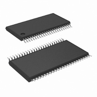
IC MCU EEPROM 8BIT 32K 48-TSSOP
Manufacturer
National Semiconductor
Series
COP8™ 8Cr
Datasheet
1.COP8CDR9HVA8NOPB.pdf
(84 pages)
Specifications of COP8CBR9IMT8/NOPB
Core Processor
COP8
Core Size
8-Bit
Speed
20MHz
Connectivity
Microwire/Plus (SPI), UART/USART
Peripherals
Brown-out Detect/Reset, POR, PWM, WDT
Number Of I /o
39
Program Memory Size
32KB (32K x 8)
Program Memory Type
FLASH
Ram Size
1K x 8
Voltage - Supply (vcc/vdd)
2.7 V ~ 5.5 V
Data Converters
A/D 16x10b
Oscillator Type
Internal
Operating Temperature
-40°C ~ 85°C
Package / Case
48-TSSOP
Data Bus Width
8 bit
Maximum Clock Frequency
20 MHz
Data Ram Size
1 KB
On-chip Adc
10 bit, 16 channel
Number Of Programmable I/os
59
Number Of Timers
3
Height
0.9 mm
Interface Type
SPI, USART
Length
12.5 mm
Maximum Operating Temperature
+ 85 C
Minimum Operating Temperature
- 40 C
Supply Voltage (max)
5.5 V
Supply Voltage (min)
2.7 V
Width
6.1 mm
Lead Free Status / RoHS Status
Lead free / RoHS Compliant
Eeprom Size
-
Lead Free Status / Rohs Status
Details
Other names
*COP8CBR9IMT8
*COP8CBR9IMT8/NOPB
COP8CBR9IMT8
*COP8CBR9IMT8/NOPB
COP8CBR9IMT8


12.0 Timers
12.2.3 Mode 2. External Event Counter Mode
This mode is quite similar to the processor independent
PWM mode described above. The main difference is that the
timer, Tx, is clocked by the input signal from the TxA pin after
synchronization to the appropriate internal clock (t
MCLK). The Tx timer control bits, TxC3, TxC2 and TxC1
allow the timer to be clocked either on a positive or negative
edge from the TxA pin. Underflows from the timer are latched
into the TxPNDA pending flag. Setting the TxENA control flag
will cause an interrupt when the timer underflows.
In this mode the input pin TxB can be used as an indepen-
dent positive edge sensitive interrupt input if the TxENB
control flag is set. The occurrence of a positive edge on the
TxB input pin is latched into the TxPNDB flag.
Figure 17 shows a block diagram of the timer in External
Event Counter mode.
Note: The PWM output is not available in this mode since the
TxA pin is being used as the counter input clock.
FIGURE 17. Timer in External Event Counter Mode
FIGURE 16. Timer in PWM Mode
(Continued)
10137420
10137419
C
or
37
12.2.4 Mode 3. Input Capture Mode
The device can precisely measure external frequencies or
time external events by placing the timer block, Tx, in the
input capture mode. In this mode, the reload registers serve
as independent capture registers, capturing the contents of
the timer when an external event occurs (transition on the
timer input pin). The capture registers can be read while
maintaining count, a feature that lets the user measure
elapsed time and time between events. By saving the timer
value when the external event occurs, the time of the exter-
nal event is recorded. Most microcontrollers have a latency
time because they cannot determine the timer value when
the external event occurs. The capture register eliminates
the latency time, thereby allowing the applications program
to retrieve the timer value stored in the capture register.
In this mode, the timer Tx is constantly running at the fixed t
or MCLK rate. The two registers, RxA and RxB, act as
capture registers. Each register also acts in conjunction with
a pin. The register RxA acts in conjunction with the TxA pin
and the register RxB acts in conjunction with the TxB pin.
The timer value gets copied over into the register when a
trigger event occurs on its corresponding pin after synchro-
nization to the appropriate internal clock (t
trol bits, TxC3, TxC2 and TxC1, allow the trigger events to be
specified either as a positive or a negative edge. The trigger
condition for each input pin can be specified independently.
The trigger conditions can also be programmed to generate
interrupts. The occurrence of the specified trigger condition
on the TxA and TxB pins will be respectively latched into the
pending flags, TxPNDA and TxPNDB. The control flag
TxENA allows the interrupt on TxA to be either enabled or
disabled. Setting the TxENA flag enables interrupts to be
generated when the selected trigger condition occurs on the
TxA pin. Similarly, the flag TxENB controls the interrupts
from the TxB pin.
Underflows from the timer can also be programmed to gen-
erate interrupts. Underflows are latched into the timer TxC0
pending flag (the TxC0 control bit serves as the timer under-
flow interrupt pending flag in the Input Capture mode). Con-
sequently, the TxC0 control bit should be reset when enter-
ing the Input Capture mode. The timer underflow interrupt is
enabled with the TxENA control flag. When a TxA interrupt
occurs in the Input Capture mode, the user must check both
the TxPNDA and TxC0 pending flags in order to determine
whether a TxA input capture or a timer underflow (or both)
caused the interrupt.
Figure 18 shows a block diagram of the timer T1 in Input
Capture mode. T2 and T3 are identical to T1.
C
or MCLK). Con-
www.national.com
C
Related parts for COP8CBR9IMT8/NOPB
Image
Part Number
Description
Manufacturer
Datasheet
Request
R

Part Number:
Description:
National Semiconductor [8-Bit D/A Converter]
Manufacturer:
National Semiconductor
Datasheet:
Part Number:
Description:
National Semiconductor [Media Coprocessor]
Manufacturer:
National Semiconductor
Datasheet:
Part Number:
Description:
Digitally Controlled Tone and Volume Circuit with Stereo Audio Power Amplifier, Microphone Preamp Stage and National 3D Sound
Manufacturer:
National Semiconductor
Datasheet:
Part Number:
Description:
Digitally Controlled Tone and Volume Circuit with Stereo Audio Power Amplifier, Microphone Preamp Stage and National 3D Sound
Manufacturer:
National Semiconductor
Datasheet:
Part Number:
Description:
AC97 Rev 2 Codec with Sample Rate Conversion and National 3D Sound
Manufacturer:
National Semiconductor
Part Number:
Description:
Manufacturer:
National Semiconductor
Datasheet:
Part Number:
Description:
Manufacturer:
National Semiconductor
Datasheet:
Part Number:
Description:
General Purpose, Low Voltage, Low Power, Rail-to-Rail Output Operational Amplifiers
Manufacturer:
National Semiconductor
Datasheet:
Part Number:
Description:
8-bit 20 MSPS flash A/D converter.
Manufacturer:
National Semiconductor
Datasheet:
Part Number:
Description:
Low Noise Quad Operational Amplifier
Manufacturer:
National Semiconductor
Datasheet:
Part Number:
Description:
Quad Differential Line Receivers
Manufacturer:
National Semiconductor
Datasheet:
Part Number:
Description:
Quad High Speed Trapezoidal? Bus Transceiver
Manufacturer:
National Semiconductor
Datasheet:
Part Number:
Description:
Dual Line Receiver
Manufacturer:
National Semiconductor
Datasheet:
Part Number:
Description:
TTL to 10k ECL Level Translator with Latch
Manufacturer:
National Semiconductor
Datasheet: