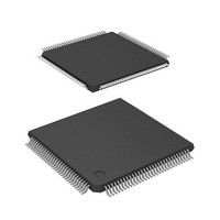
DF2367VTE33 Renesas Electronics America, DF2367VTE33 Datasheet - Page 236

DF2367VTE33
Manufacturer Part Number
DF2367VTE33
Description
IC H8S MCU FLASH 384K 120TQFP
Manufacturer
Renesas Electronics America
Series
H8® H8S/2300r
Specifications of DF2367VTE33
Core Processor
H8S/2000
Core Size
16-Bit
Speed
33MHz
Connectivity
I²C, IrDA, SCI, SmartCard
Peripherals
DMA, POR, PWM, WDT
Number Of I /o
84
Program Memory Size
384KB (384K x 8)
Program Memory Type
FLASH
Ram Size
24K x 8
Voltage - Supply (vcc/vdd)
3 V ~ 3.6 V
Data Converters
A/D 10x10b, D/A 2x8b
Oscillator Type
Internal
Operating Temperature
-20°C ~ 75°C
Package / Case
120-TQFP, 120-VQFP
Lead Free Status / RoHS Status
Contains lead / RoHS non-compliant
Eeprom Size
-
Other names
HD64F2367VTE33
HD64F2367VTE33
HD64F2367VTE33
Available stocks
Company
Part Number
Manufacturer
Quantity
Price
Company:
Part Number:
DF2367VTE33V
Manufacturer:
Renesas Electronics America
Quantity:
10 000
- Current page: 236 of 341
- Download datasheet (2Mb)
Section 2 Instruction Descriptions
2.2.60 (5)
SHLR (SHift Logical Right)
Operation
ERd (right logical shift)
Assembly-Language Format
SHLR.L ERd
Operand Size
Longword
Description
This instruction shifts the bits in a 32-bit register ERd (destination operand) one bit to the right.
The least significant bit (bit 0) shifts into the carry flag. The most significant bit (bit 31) is cleared
to 0.
Available Registers
ERd: ER0 to ER7
Operand Format and Number of States Required for Execution
Notes
Rev. 4.00 Feb 24, 2006 page 220 of 322
REJ09B0139-0400
Register direct
Addressing
Mode
SHLR (L)
Mnemonic
0
SHLR.L
MSB
b31
ERd
Operands
ERd
.
. . . . . .
.
1st byte
1
.
.
1
Condition Code
H: Previous value remains unchanged.
N: Always cleared to 0.
Z: Set to 1 if the result is zero; otherwise
V: Always cleared to 0.
C: Receives the previous value in bit 0.
.
2nd byte
3
.
Instruction Format
cleared to 0.
—
I
0 erd
UI H
—
LSB
b0
—
3rd byte
—
U
C
N
0
4th byte
Z
Shift Logical
V
0
States
No. of
C
1
Related parts for DF2367VTE33
Image
Part Number
Description
Manufacturer
Datasheet
Request
R

Part Number:
Description:
CONN PLUG 12POS DUAL 0.5MM SMD
Manufacturer:
Hirose Electric Co Ltd
Datasheet:

Part Number:
Description:
CONN PLUG 18POS DUAL 0.5MM SMD
Manufacturer:
Hirose Electric Co Ltd
Datasheet:

Part Number:
Description:
CONN PLUG 14POS DUAL 0.5MM SMD
Manufacturer:
Hirose Electric Co Ltd
Datasheet:

Part Number:
Description:
CONN RECEPT 20POS DUAL 0.5MM SMD
Manufacturer:
Hirose Electric Co Ltd
Datasheet:

Part Number:
Description:
CONN PLUG 16POS DUAL 0.5MM SMD
Manufacturer:
Hirose Electric Co Ltd
Datasheet:

Part Number:
Description:
CONN RECEPT 16POS DUAL 0.5MM SMD
Manufacturer:
Hirose Electric Co Ltd
Datasheet:

Part Number:
Description:
CONN PLUG 20POS DUAL 0.5MM SMD
Manufacturer:
Hirose Electric Co Ltd
Datasheet:

Part Number:
Description:
CONN PLUG 30POS DUAL 0.5MM SMD
Manufacturer:
Hirose Electric Co Ltd
Datasheet:

Part Number:
Description:
CONN RECEPT 30POS DUAL 0.5MM SMD
Manufacturer:
Hirose Electric Co Ltd
Datasheet:

Part Number:
Description:
CONN PLUG 40POS DUAL 0.5MM SMD
Manufacturer:
Hirose Electric Co Ltd
Datasheet:

Part Number:
Description:
KIT STARTER FOR M16C/29
Manufacturer:
Renesas Electronics America
Datasheet:

Part Number:
Description:
KIT STARTER FOR R8C/2D
Manufacturer:
Renesas Electronics America
Datasheet:

Part Number:
Description:
R0K33062P STARTER KIT
Manufacturer:
Renesas Electronics America
Datasheet:

Part Number:
Description:
KIT STARTER FOR R8C/23 E8A
Manufacturer:
Renesas Electronics America
Datasheet:

Part Number:
Description:
KIT STARTER FOR R8C/25
Manufacturer:
Renesas Electronics America
Datasheet:


