M30873FHGP#U5 Renesas Electronics America, M30873FHGP#U5 Datasheet - Page 527
M30873FHGP#U5
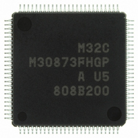
Manufacturer Part Number
M30873FHGP#U5
Description
IC M32C/87 MCU FLASH 100LQFP
Manufacturer
Renesas Electronics America
Series
M16C™ M32C/80r
Datasheet
1.M3087BFLGPU3.pdf
(629 pages)
Specifications of M30873FHGP#U5
Core Processor
M32C/80
Core Size
16/32-Bit
Speed
32MHz
Connectivity
CAN, EBI/EMI, I²C, IEBus, IrDA, SIO, UART/USART
Peripherals
DMA, POR, PWM, WDT
Number Of I /o
85
Program Memory Size
384KB (384K x 8)
Program Memory Type
FLASH
Ram Size
24K x 8
Voltage - Supply (vcc/vdd)
3 V ~ 5.5 V
Data Converters
A/D 26x10b; D/A 2x8b
Oscillator Type
Internal
Operating Temperature
-20°C ~ 85°C
Package / Case
100-LQFP
For Use With
R0K330879S001BE - KIT DEV RSK M32C/87R0K330879S000BE - KIT DEV RSK M32C/87
Lead Free Status / RoHS Status
Lead free / RoHS Compliant
Eeprom Size
-
Available stocks
Company
Part Number
Manufacturer
Quantity
Price

Part Number:
M30873FHGP#U5M30873FHGP#U3
Manufacturer:
Renesas Electronics America
Quantity:
10 000


M32C/87 Group (M32C/87, M32C/87A, M32C/87B)
REJ09B0180-0151 Rev.1.51 Jul 31, 2008
Page 503 of 587
Figure 26.8
<Low-power consumption mode program>
Execute the following procedure using the program for low-power
consumption mode transferred to an area other than the flash memory
Transfer the program for low-power consumption mode
Jump to the program for low-power consumption mode
transferred to an area other than the flash memory.
FMR0 register: FMR01 bit = 0
FMR0 register: FMR01 bit = 1
FMR0 register: FMSTP bit = 1
Switch the CPU clock source
Stop main clock
Oscillate main clock
Switch the CPU clock source
FMR0 register: FMSTP bit = 0
FMR0 register: FMR01 bit = 0
Jump to a given address in the flash memory
to an area other than the flash memory
Processing in low-power consumption
mode or on-chip oscillator low-power
Setting Procedure to Enter and Exit Low Power Mode
consumption mode
Wait for tps
Start
End
CPU rewrite mode enabled
- To set the FMR01 bit to 1, write a 1 to the FMR01 bit
- Set it while "H" is applied to the NMI pin.
Flash memory stops operating
(Enters low-power consumption state and a flash memory is initialized)
When switching the CPU clock source, wait until the new CPU clock
source stabilizes.
Flash memory starts operating
CPU rewrite mode disabled
-
Wait time to stabilize flash memory circuit
- Add tps wait time by a program.
- Do not access the flash memory during this wait time.
To change the FMR01 bit from 1 to 0, enter read array mode
immediately after writing a 0.
Write the value to the FMR0 register in 8-bit units.
Do not generate an interrupt or a DMA or DMACII transfer
between these two settings.
and then write to address 0057h in 16-bit units.
Set the eight high-order bits to 00h.
26. Flash Memory
Related parts for M30873FHGP#U5
Image
Part Number
Description
Manufacturer
Datasheet
Request
R

Part Number:
Description:
KIT STARTER FOR M16C/29
Manufacturer:
Renesas Electronics America
Datasheet:

Part Number:
Description:
KIT STARTER FOR R8C/2D
Manufacturer:
Renesas Electronics America
Datasheet:

Part Number:
Description:
R0K33062P STARTER KIT
Manufacturer:
Renesas Electronics America
Datasheet:

Part Number:
Description:
KIT STARTER FOR R8C/23 E8A
Manufacturer:
Renesas Electronics America
Datasheet:

Part Number:
Description:
KIT STARTER FOR R8C/25
Manufacturer:
Renesas Electronics America
Datasheet:

Part Number:
Description:
KIT STARTER H8S2456 SHARPE DSPLY
Manufacturer:
Renesas Electronics America
Datasheet:

Part Number:
Description:
KIT STARTER FOR R8C38C
Manufacturer:
Renesas Electronics America
Datasheet:

Part Number:
Description:
KIT STARTER FOR R8C35C
Manufacturer:
Renesas Electronics America
Datasheet:

Part Number:
Description:
KIT STARTER FOR R8CL3AC+LCD APPS
Manufacturer:
Renesas Electronics America
Datasheet:
Part Number:
Description:
KIT STARTER FOR RX610
Manufacturer:
Renesas Electronics America
Datasheet:

Part Number:
Description:
KIT STARTER FOR R32C/118
Manufacturer:
Renesas Electronics America
Datasheet:

Part Number:
Description:
KIT DEV RSK-R8C/26-29
Manufacturer:
Renesas Electronics America
Datasheet:

Part Number:
Description:
KIT STARTER FOR SH7124
Manufacturer:
Renesas Electronics America
Datasheet:

Part Number:
Description:
KIT STARTER FOR H8SX/1622
Manufacturer:
Renesas Electronics America
Datasheet:

Part Number:
Description:
KIT DEV FOR SH7203
Manufacturer:
Renesas Electronics America
Datasheet: