DS80C310-ECG Maxim Integrated Products, DS80C310-ECG Datasheet - Page 5
DS80C310-ECG
Manufacturer Part Number
DS80C310-ECG
Description
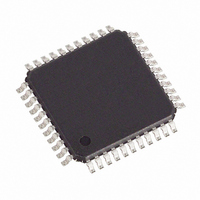
IC MCU HI SPEED 25MHZ 44-TQFP
Manufacturer
Maxim Integrated Products
Series
80Cr
Datasheet
1.DS80C310FCG.pdf
(22 pages)
Specifications of DS80C310-ECG
Core Processor
8051
Core Size
8-Bit
Speed
25MHz
Connectivity
EBI/EMI, SIO, UART/USART
Peripherals
Brown-out Detect/Reset, POR
Number Of I /o
32
Program Memory Type
ROMless
Ram Size
256 x 8
Voltage - Supply (vcc/vdd)
4.5 V ~ 5.5 V
Oscillator Type
External
Operating Temperature
0°C ~ 70°C
Package / Case
44-TQFP, 44-VQFP
Processor Series
DS80C310
Core
8051
Data Bus Width
8 bit
Program Memory Size
64 KB
Data Ram Size
64 KB
Interface Type
UART
Maximum Clock Frequency
25 MHz
Number Of Programmable I/os
32
Number Of Timers
3
Operating Supply Voltage
4.5 V to 5.5 V
Maximum Operating Temperature
+ 70 C
Mounting Style
SMD/SMT
3rd Party Development Tools
PK51, CA51, A51, ULINK2
Minimum Operating Temperature
0 C
Lead Free Status / RoHS Status
Contains lead / RoHS non-compliant
Eeprom Size
-
Program Memory Size
-
Data Converters
-
Available stocks
Company
Part Number
Manufacturer
Quantity
Price
Company:

Part Number:
DS80C310-ECG
Manufacturer:
Maxim Integrated
Quantity:
10 000
Company:
Part Number:
DS80C310-ECG+
Manufacturer:
Microchip
Quantity:
461
Company:
Part Number:
DS80C310-ECG+
Manufacturer:
Maxim Integrated
Quantity:
10 000


COMPATIBILITY
The DS80C310 is a fully static, CMOS, 8051-compatible microcontroller designed for high performance.
In most cases the DS80C310 can drop into an existing socket for the 80C31 or 80C32 to significantly
improve the operation. In general, software written for existing 8051-based systems works without
modification on the DS80C310. The exception is critical timing because the high-speed microcontroller
performs its instructions much faster than the original for any given crystal selection. The DS80C310 runs
the standard 8051 family instruction set and is pin compatible with DIP, PLCC, or TQFP packages. The
DS80C310 is a streamlined version of the DS80C320. It maintains upward compatibility but has fewer
peripherals.
The DS80C310 provides three 16-bit timer/counters, a full-duplex serial port, and 256 bytes of direct
RAM. I/O ports have the same operation as a standard 8051 product. Timers default to a 12 clock-per-
cycle operation to keep their timing compatible with original 8051 family systems. However, timers are
individually programmable to run at the new 4 clocks per cycle if desired.
The DS80C310 provides several new hardware functions that are controlled by Special Function
Registers (SFRs). Table 1 summarizes the SFRs.
PERFORMANCE OVERVIEW
The DS80C310 features a high-speed 8051-compatible core. Higher speed comes not just from increasing
the clock frequency but from a newer, more efficient design.
This updated core does not have the dummy memory cycles that exist in a standard 8051. A conventional
8051 generates machine cycles using the clock frequency divided by 12. In the DS80C310, the same
PDIP
29
30
31
32
33
34
35
36
37
38
39
40
–
PLCC
12, 34
PIN
32
33
35
36
37
38
39
40
41
42
43
44
TQFP
6, 28
26
27
29
30
31
32
33
34
35
36
37
38
AD7 (P0.7)
AD6 (P0.6)
AD5 (P0.5)
AD4 (P0.4)
AD3 (P0.3)
AD2 (P0.2)
AD1 (P0.1)
AD0 (P0.0)
NAME
PSEN
ALE
N.C.
V
EA
CC
Active-Low Program Store Enable (Output). This signal is
commonly connected to external ROM memory as a chip enable.
PSEN is driven high when data memory (RAM) is being accessed
through the bus and during a reset condition.
Address Latch Enable (Output). The output functions as clock to
latch the external address LSB from the multiplexed address/data
bus on Port 0. This signal is commonly connected to the latch enable
of an external 373 family transparent latch. ALE is forced high when
the DS80C310 is in a reset condition.
Active-Low External Access (Input). This pin must be connected to
ground for proper operation.
Address/Data Bus 0–7 (Port 0) (I/O). Port 0 is the multiplexed
address/data bus. During the time when ALE is high, the LSB of a
memory address is presented. When ALE falls to logic 0, the port
transitions to a bidirectional data bus. This bus is used to read
external ROM and read/write external RAM memory or peripherals.
Port 0 has no true port latch and cannot be written directly by
software. The reset condition of Port 0 is high.
+5V Power Supply
No Connection (Reserved). These pins should not be connected.
They are reserved for use with future devices in this family.
5 of 22
FUNCTION
DS80C310
Related parts for DS80C310-ECG
Image
Part Number
Description
Manufacturer
Datasheet
Request
R

Part Number:
Description:
Manufacturer:
Maxim Integrated Products
Datasheet:

Part Number:
Description:
IC MCU HI SPEED 25MHZ 44-TQFP
Manufacturer:
Maxim Integrated Products
Datasheet:

Part Number:
Description:
IC MCU HI SPEED 25MHZ IND 44PLCC
Manufacturer:
Maxim Integrated Products
Datasheet:
Part Number:
Description:
IC MCU HI SPEED 25MHZ 44-PLCC
Manufacturer:
Maxim Integrated Products
Datasheet:

Part Number:
Description:
IC MCU HI SPEED 25MHZ 40-DIP
Manufacturer:
Maxim Integrated Products
Datasheet:
Part Number:
Description:
IC MCU HI SPEED 25MHZ 44-PLCC
Manufacturer:
Maxim Integrated Products
Datasheet:
Part Number:
Description:
IC MCU HI SPEED 25MHZ 44-PLCC
Manufacturer:
Maxim Integrated Products
Datasheet:
Part Number:
Description:
IC MCU HI SPEED 25MHZ IND 44PLCC
Manufacturer:
Maxim Integrated Products
Datasheet:

Part Number:
Description:
IC MCU HI SPEED 25MHZ 44-MQFP
Manufacturer:
Maxim Integrated Products
Datasheet:
Part Number:
Description:
IC MCU HI SPEED 25MHZ 44-PLCC
Manufacturer:
Maxim Integrated Products
Datasheet:
Part Number:
Description:
IC MCU HI SPEED 25MHZ 40-DIP
Manufacturer:
Maxim Integrated Products
Datasheet:
Part Number:
Description:
IC MCU HI SPEED 25MHZ IND 44PLCC
Manufacturer:
Maxim Integrated Products
Datasheet:
Part Number:
Description:
IC MCU HI SPEED 25MHZ 44-MQFP
Manufacturer:
Maxim Integrated Products
Datasheet:
Part Number:
Description:
IC MCU HI SPEED 25MHZ 44-MQFP
Manufacturer:
Maxim Integrated Products
Datasheet:
Part Number:
Description:
MAX7528KCWPMaxim Integrated Products [CMOS Dual 8-Bit Buffered Multiplying DACs]
Manufacturer:
Maxim Integrated Products
Datasheet: