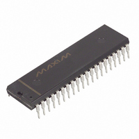
DS89C450-MNL Maxim Integrated Products, DS89C450-MNL Datasheet - Page 21

DS89C450-MNL
Manufacturer Part Number
DS89C450-MNL
Description
IC MCU FLASH 64KB 33MHZ 40-DIP
Manufacturer
Maxim Integrated Products
Series
89Cr
Datasheet
1.DS89C450-KIT.pdf
(46 pages)
Specifications of DS89C450-MNL
Core Processor
8051
Core Size
8-Bit
Speed
33MHz
Connectivity
EBI/EMI, SIO, UART/USART
Peripherals
Power-Fail Reset, WDT
Number Of I /o
32
Program Memory Size
64KB (64K x 8)
Program Memory Type
FLASH
Ram Size
1K x 8
Voltage - Supply (vcc/vdd)
4.5 V ~ 5.5 V
Oscillator Type
External
Operating Temperature
-40°C ~ 85°C
Package / Case
40-DIP (0.600", 15.24mm)
Processor Series
DS89C450
Core
8051
Data Bus Width
8 bit
Data Ram Size
1 KB
Interface Type
UART
Maximum Clock Frequency
33 MHz
Number Of Programmable I/os
4
Number Of Timers
3
Operating Supply Voltage
4.5 V to 5.5 V
Maximum Operating Temperature
+ 85 C
Mounting Style
Through Hole
3rd Party Development Tools
PK51, CA51, A51, ULINK2
Development Tools By Supplier
DS89C450-KIT#
Minimum Operating Temperature
- 40 C
Lead Free Status / RoHS Status
Contains lead / RoHS non-compliant
Eeprom Size
-
Data Converters
-
Available stocks
Company
Part Number
Manufacturer
Quantity
Price
Company:
Part Number:
DS89C450-MNL+
Manufacturer:
AD
Quantity:
101
Program Memory Access
On-chip program memory begins at address 0000h and is contiguous through 3FFFh (16kB) on the DS89C430 and
through FFFFh (64kB) on the DS89C450. Exceeding the maximum address of on-chip program memory causes
the device to access off-chip memory. The maximum on-chip decoded address is selectable by software using the
ROMSIZE feature. Software can cause the DS89C430 to behave like a device with less on-chip memory. This is
beneficial when overlapping external memory is used. The maximum memory size is dynamically variable. Thus a
portion of memory can be removed from the memory map to access off-chip memory and then be restored to
access on-chip memory. In fact, all the on-chip memory can be removed from the memory map allowing the full
64kB memory space to be addressed from off-chip memory. Program memory addresses that are larger than the
selected maximum are automatically fetched from outside the part through ports 0 and 2.
depiction of the memory map.
The ROMSIZE register is used to select the maximum on-chip decoded address for program memory. Bits RMS2,
RMS1, and RMS0 have the following effect:
The reset default condition for all devices is to their maximum on-chip program memory size. When accessing
external program memory, that amount of external memory would be inaccessible. To select a smaller effective
program memory size, software must alter bits RMS2–RMS0. Altering these bits requires a timed-access
procedure, as explained later.
Care should be taken so that changing the ROMSIZE register does not corrupt program execution. For example,
assume that a DS89C430 is executing instructions from internal program memory near the 12kB boundary
(~3000h) and that the ROMSIZE register is currently configured for a 16kB internal program space. If software
reconfigures the ROMSIZE register to 4kB (0000h–0FFFh) in the current state, the device immediately jumps to
external program execution because program code from 4kB to 16kB (1000h–3FFFh) is no longer located on-chip.
This could result in code misalignment and execution of an invalid instruction. The recommended method is to
modify the ROMSIZE register from a location in memory that is internal (or external) both before and after the
operation. In the above example, the instruction that modifies the ROMSIZE register should be located below the
4kB (1000h) boundary or above the 16kB (3FFFh) boundary so that it is unaffected by the memory modification.
The same precaution should be applied if the internal program memory size is modified while executing from
external program memory.
For nonpage mode operations, off-chip memory is accessed using the multiplexed address/data bus on P0 and the
MSB address on P2. While serving as a memory bus, these pins are not I/O ports. This convention follows the
standard 8051 method of expanding on-chip memory. Off-chip program memory access also occurs if the EA pin is
a logic 0. EA overrides all ROMSIZE bit settings. The PSEN signal goes active (low) to serve as a chip enable or
output enable when ports 0 and 2 fetch from external program memory.
The RD and WR signals are used to control the external data memory device. Data memory is accessed by MOVX
instructions. The MOVX@Ri instruction uses the value in the designated working register to provide the LSB of the
address, while port 2 supplies the address MSB. The MOVX@DPTR instruction uses one of the two data pointers
to move data over the entire 64kB external data memory space. Software selects the data pointer used by writing
to the SEL bit (DPS.0).
The DS89C430 also provides a user option for high-speed external memory access by reconfiguring the external
memory interface into page mode operation.
Note: When using the original 8051 expanded bus structure, the throughput is reduced by 75% compared with that
of internal operations. This is because of the CPU being stalled for three out of four clocks, waiting for the data
RMS2
0
0
0
0
1
1
1
1
RMS1
1
0
0
1
0
0
1
1
RMS0
0
1
0
1
0
1
0
1
DS89C430/DS89C450 Ultra-High-Speed Flash Microcontrollers
Maximum On-Chip Program Memory Address
21 of 46
16kB/3FFFh (DS89C430 default)
64kB/FFFFh (DS89C450 default)
(Size/Address)
32kB/7FFFh
4kB/0FFFh
8kB/1FFFh
1kB/03FFh
2kB/07FFh
0kB
Figure 6
shows a


