PIC17C42-25/JW Microchip Technology, PIC17C42-25/JW Datasheet - Page 42
PIC17C42-25/JW
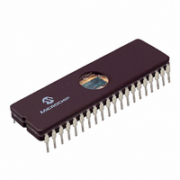
Manufacturer Part Number
PIC17C42-25/JW
Description
MICRO CTRL 2K X 16 EPROM 40 CDIP
Manufacturer
Microchip Technology
Series
PIC® 17Cr
Specifications of PIC17C42-25/JW
Core Processor
PIC
Core Size
8-Bit
Speed
25MHz
Connectivity
UART/USART
Peripherals
POR, PWM, WDT
Number Of I /o
33
Program Memory Size
4KB (2K x 16)
Program Memory Type
EPROM, UV
Ram Size
232 x 8
Voltage - Supply (vcc/vdd)
4.5 V ~ 5.5 V
Oscillator Type
External
Operating Temperature
0°C ~ 70°C
Package / Case
40-CDIP (0.600", 15.24mm) Window
For Use With
AC174001 - MODULE SKT PROMATEII 40DIP
Lead Free Status / RoHS Status
Contains lead / RoHS non-compliant
Eeprom Size
-
Data Converters
-
Other names
PIC17C42/JW


PIC17C4X
6.8
The BSR is used to switch between banks in the data
memory
PIC17CR42, and PIC17C42A only the lower nibble is
implemented. While in the PIC17C43, PIC17CR43,
and PIC17C44 devices, the entire byte is implemented.
The lower nibble is used to select the peripheral regis-
ter bank. The upper nibble is used to select the general
purpose memory bank.
All the Special Function Registers (SFRs) are mapped
into the data memory space. In order to accommodate
the large number of registers, a banking scheme has
been used. A segment of the SFRs, from address 10h
to address 17h, is banked. The lower nibble of the bank
select register (BSR) selects the currently active
“peripheral bank.” Effort has been made to group the
peripheral registers of related functionality in one bank.
However, it will still be necessary to switch from bank
to bank in order to address all peripherals related to a
single task. To assist this, a MOVLB bank instruction is
in the instruction set.
FIGURE 6-13: BSR OPERATION (PIC17C43/R43/44)
DS30412C-page 42
Note 1:
Address
Range
10h
17h
20h
FFh
2: Only Banks 0 and Bank 1 are implemented. Selection of an unimplemented bank is not recommended.
BSR
7
Bank Select Register (BSR)
area
Bank 15 is reserved for Microchip use, reading of registers in this bank may cause random values to be read.
Only Banks 0 through Bank 3 are implemented. Selection of an unimplemented bank is not recommended.
(2)
4 3
(Figure 6-13). In
(1)
Bank 0
Bank 0
0
0
0
Bank 1
Bank 1
1
1
the
Bank 2
Bank 2
PIC17C42,
2
2
Bank 3
3
For the PIC17C43, PIC17CR43, and PIC17C44
devices, the need for a large general purpose memory
space dictated a general purpose RAM banking
scheme. The upper nibble of the BSR selects the cur-
rently active general purpose RAM bank. To assist this,
a MOVLR bank instruction has been provided in the
instruction set.
If the currently selected bank is not implemented (such
as Bank 13), any read will read all '0's. Any write is com-
pleted to the bit bucket and the ALU status bits will be
set/cleared as appropriate.
Bank 4
Note:
4
Registers in Bank 15 in the Special Func-
tion Register area, are reserved for
Microchip use. Reading of registers in this
bank may cause random values to be read.
Bank 15
Bank 15
1996 Microchip Technology Inc.
15
15
SFR
Banks
GPR
Banks
Related parts for PIC17C42-25/JW
Image
Part Number
Description
Manufacturer
Datasheet
Request
R

Part Number:
Description:
High-Performance 8-Bit CMOS EPROM/ROM Microcontroller
Manufacturer:
Microchip Technology
Datasheet:

Part Number:
Description:
Manufacturer:
Microchip Technology Inc.
Datasheet:
Part Number:
Description:
Manufacturer:
Microchip Technology Inc.
Datasheet:
Part Number:
Description:
Manufacturer:
Microchip Technology Inc.
Datasheet:
Part Number:
Description:
Manufacturer:
Microchip Technology Inc.
Datasheet:
Part Number:
Description:
Manufacturer:
Microchip Technology Inc.
Datasheet:
Part Number:
Description:
Manufacturer:
Microchip Technology Inc.
Datasheet:
Part Number:
Description:
Manufacturer:
Microchip Technology Inc.
Datasheet:
Part Number:
Description:
Manufacturer:
Microchip Technology Inc.
Datasheet: