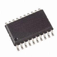
AT90S2313-4SI Atmel, AT90S2313-4SI Datasheet - Page 61

AT90S2313-4SI
Manufacturer Part Number
AT90S2313-4SI
Description
MCU 2K FLASH 4MHZ 20-SOIC
Manufacturer
Atmel
Series
AVR® 90Sr
Datasheet
1.AT90S2313-10PC.pdf
(92 pages)
Specifications of AT90S2313-4SI
Core Processor
AVR
Core Size
8-Bit
Speed
4MHz
Connectivity
SPI, UART/USART
Peripherals
Brown-out Detect/Reset, POR, PWM, WDT
Number Of I /o
15
Program Memory Size
2KB (1K x 16)
Program Memory Type
FLASH
Eeprom Size
128 x 8
Ram Size
128 x 8
Voltage - Supply (vcc/vdd)
2.7 V ~ 6 V
Oscillator Type
External
Operating Temperature
-40°C ~ 85°C
Package / Case
20-SOIC (7.5mm Width)
Data Bus Width
8 bit
Data Ram Size
128 B
Interface Type
SPI, UART
Maximum Clock Frequency
4 MHz
Number Of Programmable I/os
15
Number Of Timers
1 x 8 bit
Operating Supply Voltage
2.7 V to 6 V
Maximum Operating Temperature
+ 85 C
Mounting Style
SMD/SMT
Minimum Operating Temperature
- 40 C
Lead Free Status / RoHS Status
Contains lead / RoHS non-compliant
Data Converters
-
Lead Free Status / Rohs Status
No
Available stocks
Company
Part Number
Manufacturer
Quantity
Price
Part Number:
AT90S2313-4SI
Manufacturer:
ATMEL/爱特梅尔
Quantity:
20 000
Parallel Programming
Signal Names
0839I–AVR–06/02
within the self-timed write instruction in the Serial Programming mode. During program-
ming, the supply voltage must be in accordance with Table 22.
Table 22. Supply Voltage during Programming
This section describes how to parallel program and verify Flash Program memory,
EEPROM data memory, Lock bits and Fuse bits in the AT90S2313.
In this section, some pins of the AT90S2313 are referenced by signal names describing
their function during parallel programming. Pins not described in the following table are
referenced by pin names. See Figure 49 and Table 23. Pins not described in Table 23
are referenced by pin names.
The XA1/XA0 pins determine the action executed when the XTAL1 pin is given a posi-
tive pulse. The bit coding is shown in Table 24.
When pulsing WR or OE, the command loaded determines the action executed. The
command is a byte where the different bits are assigned functions as shown in Table 25.
Figure 49. Parallel Programming
.
Table 23. Pin Name Mapping
Part
AT90S2313
Programming Mode
Signal Name in
RDY/BSY
WR
OE
BS
Pin Name
PD1
PD2
PD3
PD4
Serial Programming
2.7 - 6.0V
I/O
O
I
I
I
Function
0: Device is busy programming, 1: Device is ready
for new command
Output Enable (Active low)
Write Pulse (Active low)
Byte Select (“0” selects low byte, “1” selects high
byte)
Parallel Programming
4.5 - 5.5V
AT90S2313
61


