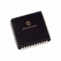
PIC16C662-20I/L Microchip Technology, PIC16C662-20I/L Datasheet - Page 41

PIC16C662-20I/L
Manufacturer Part Number
PIC16C662-20I/L
Description
IC MCU OTP 4KX14 COMP 44PLCC
Manufacturer
Microchip Technology
Series
PIC® 16Cr
Specifications of PIC16C662-20I/L
Core Processor
PIC
Core Size
8-Bit
Speed
20MHz
Peripherals
Brown-out Detect/Reset, LED, POR, WDT
Number Of I /o
33
Program Memory Size
7KB (4K x 14)
Program Memory Type
OTP
Ram Size
176 x 8
Voltage - Supply (vcc/vdd)
4 V ~ 6 V
Oscillator Type
External
Operating Temperature
-40°C ~ 85°C
Package / Case
44-PLCC
Processor Series
PIC16C
Core
PIC
Data Bus Width
8 bit
Data Ram Size
176 B
Interface Type
RS- 232
Maximum Clock Frequency
20 MHz
Number Of Programmable I/os
33
Number Of Timers
8
Operating Supply Voltage
3 V to 6 V
Maximum Operating Temperature
+ 85 C
Mounting Style
SMD/SMT
3rd Party Development Tools
52715-96, 52716-328, 52717-734
Development Tools By Supplier
ICE2000, DM163022
Minimum Operating Temperature
- 40 C
On-chip Adc
10 bit
For Use With
DVA16XL441 - ADAPTER DEVICE ICE 44PLCC309-1040 - ADAPTER 44-PLCC ZIF TO 40-DIP309-1039 - ADAPTER 44-PLCC TO 40-DIP
Lead Free Status / RoHS Status
Lead free / RoHS Compliant
Eeprom Size
-
Data Converters
-
Connectivity
-
Lead Free Status / Rohs Status
Details
Available stocks
Company
Part Number
Manufacturer
Quantity
Price
Company:
Part Number:
PIC16C662-20I/L
Manufacturer:
Microchip Technology
Quantity:
10 000
6.0
The Timer0 module has the following features:
• 8-bit timer/counter register, TMR0
• 8-bit software programmable prescaler
• Internal or external clock select
Figure 6-1 is a simplified block diagram of the Timer0
module.
Timer mode is selected by clearing bit T0CS
(OPTION<5>). In timer mode, the Timer0 module will
increment every instruction cycle (without prescaler). If
TMR0 register is written, the increment is inhibited for
the following two instruction cycles (Figure 6-2 and
Figure 6-3). The user can work around this by writing
an adjusted value to the TMR0 register.
Counter mode is selected by setting bit T0CS. In this
mode, Timer0 will increment either on every rising or
falling edge of pin RA4/T0CKI. The incrementing edge
is determined by the source edge select bit T0SE
FIGURE 6-1:
FIGURE 6-2:
1996 Microchip Technology Inc.
- Read and write capability
- Interrupt on overflow from FFh to 00h
- Edge select for external clock
Instruction
TMR0
PC
(Program
Counter)
Fetch
RA4/T0CKI
pin
Instruction
Executed
Note 1:
TIMER0 MODULE
2: The prescaler is shared with Watchdog Timer (refer to Figure 6-6 for detailed diagram).
T0SE
Bits, T0CS, T0SE, PSA, and PS2, PS1, PS0 are (OPTION<5:0).
Q1 Q2 Q3 Q4 Q1 Q2 Q3 Q4 Q1 Q2 Q3 Q4 Q1 Q2 Q3 Q4 Q1 Q2 Q3 Q4 Q1 Q2 Q3 Q4 Q1 Q2 Q3 Q4 Q1 Q2 Q3 Q4
T0
F
TIMER0 BLOCK DIAGRAM
TIMER0 TIMING: INTERNAL CLOCK/NO PRESCALER
OSC
PC-1
/4
MOVWF TMR0
T0+1
This document was created with FrameMaker 4 0 4
T0CS
PC
0
1
MOVF TMR0,W MOVF TMR0,W MOVF TMR0,W MOVF TMR0,W
T0+2
Write TMR0
executed
PS2, PS1, PS0
Programmable
PC+1
Prescaler
3
Preliminary
PIC16C64X & PIC16C66X
NT0
Read TMR0
reads NT0
PC+2
PSA
1
0
(OPTION<4>). Clearing bit T0SE selects the rising
edge. Restrictions on the external clock input are dis-
cussed in detail in Section 6.2.
The prescaler is mutually exclusively shared between
the Timer0 module and the Watchdog Timer. The pres-
caler assignment is controlled in software by control bit
PSA (OPTION<3>). Clearing bit PSA will assign the
prescaler to the Timer0 module. The prescaler is not
readable or writable. When the prescaler is assigned to
the Timer0 module, prescale values of 1:2, 1:4, …,
1:256 are selectable. Section 6.3 details the operation
of the prescaler.
6.1
The TMR0 interrupt is generated when the register
(TMR0) overflows from FFh to 00h. This overflow sets
interrupt flag bit T0IF (INTCON<2>). The interrupt can
be masked by clearing enable bit T0IE (INTCON<5>).
Flag bit T0IF must be cleared in software by the Timer0
interrupt service routine before re-enabling this inter-
rupt. The TMR0 interrupt cannot wake the processor
from SLEEP since the timer is shut off during SLEEP.
Figure 6-4 displays the Timer0 interrupt timing.
PSout
Read TMR0
reads NT0
NT0
PC+3
(2 cycle delay)
Sync with
Timer0 Interrupt
Internal
clocks
Read TMR0
reads NT0
NT0
PC+4
PSout
MOVF TMR0,W
Read TMR0
reads NT0 + 1
TMR0 reg
NT0+1
Data bus
PC+5
8
DS30559A-page 41
Read TMR0
reads NT0 + 2
Set bit T0IF
on overflow
NT0+2
PC+6


