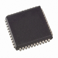
AT87F55WD-24AC Atmel, AT87F55WD-24AC Datasheet - Page 3

AT87F55WD-24AC
Manufacturer Part Number
AT87F55WD-24AC
Description
IC MICRO CTRL 24MHZ 44PLCC
Manufacturer
Atmel
Series
87Fr
Datasheet
1.AT87F55WD-24AC.pdf
(26 pages)
Specifications of AT87F55WD-24AC
Core Processor
8051
Core Size
8-Bit
Speed
24MHz
Connectivity
UART/USART
Peripherals
WDT
Number Of I /o
32
Program Memory Size
20KB (20K x 8)
Program Memory Type
OTP Quick FLASH
Ram Size
256 x 8
Voltage - Supply (vcc/vdd)
4 V ~ 5.5 V
Oscillator Type
Internal
Operating Temperature
0°C ~ 70°C
Package / Case
44-PLCC
Lead Free Status / RoHS Status
Contains lead / RoHS non-compliant
Eeprom Size
-
Data Converters
-
Other names
AT87F55WD24AC
The AT87F55WD provides the following standard features:
20K bytes of QuickFlash, 256 bytes of RAM, 32 I/O lines,
three 16-bit timer/counters, a six-vector, two-level interrupt
architecture, a full-duplex serial port, on-chip oscillator, and
clock circuitry. In addition, the AT87F55WD is designed
with static logic for operation down to zero frequency and
supports two software selectable power saving modes. The
Idle Mode stops the CPU while allowing the RAM,
timer/counters, serial port, and interrupt system to continue
functioning. The Power-down mode saves the RAM con-
tents but freezes the oscillator, disabling all other chip func-
tions until the next external interrupt or hardware reset.
Pin Description
VCC
Supply voltage.
GND
Ground.
Port 0
Port 0 is an 8-bit open-drain bidirectional I/O port. As an
output port, each pin can sink eight TTL inputs. When 1s
are written to port 0 pins, the pins can be used as high-
impedance inputs.
Port 0 can also be configured to be the multiplexed low-
order address/data bus during accesses to external
program and data memory. In this mode, P0 has internal
pullups.
Port 0 also receives the code bytes during QuickFlash pro-
gramming and outputs the code bytes during program veri-
fication. External pullups are required during program
verification.
Port 1
Port 1 is an 8-bit bidirectional I/O port with internal pullups.
The Port 1 output buffers can sink/source four TTL inputs.
When 1s are written to Port 1 pins, they are pulled high by
the internal pullups and can be used as inputs. As inputs,
Port 1 pins that are externally being pulled low will source
current (I
In addition, P1.0 and P1.1 can be configured to be the
timer/counter 2 external count input (P1.0/T2) and the
timer/counter 2 trigger input (P1.1/T2EX), respectively, as
shown in the following table.
Port 1 also receives the low-order address bytes during
QuickFlash programming and verification.
Port Pin
P1.0
P1.1
IL
) because of the internal pullups.
Alternate Functions
T2 (external count input to Timer/Counter 2),
clock-out
T2EX (Timer/Counter 2 capture/reload trigger
and direction control)
Port 2
Port 2 is an 8-bit bidirectional I/O port with internal pullups.
The Port 2 output buffers can sink/source four TTL inputs.
When 1s are written to Port 2 pins, they are pulled high by
the internal pullups and can be used as inputs. As inputs,
Port 2 pins that are externally being pulled low will source
current (I
Port 2 emits the high-order address byte during fetches
from external program memory and during accesses to
external data memory that use 16-bit addresses (MOVX @
DPTR). In this application, Port 2 uses strong internal pul-
lups when emitting 1s. During accesses to external data
memory that use 8-bit addresses (MOVX @ RI), Port 2
emits the contents of the P2 Special Function Register.
Port 2 also receives the high-order address bits and some
control signals during QuickFlash programming and verifi-
cation.
Port 3
Port 3 is an 8-bit bidirectional I/O port with internal pullups.
The Port 3 output buffers can sink/source four TTL inputs.
When 1s are written to Port 3 pins, they are pulled high by
the internal pullups and can be used as inputs. As inputs,
Port 3 pins that are externally being pulled low will source
current (I
Port 3 also serves the functions of various special features
of the AT87F55WD, as shown in the following table.
Port 3 also receives some control signals for QuickFlash
programming and verification.
RST
Reset input. A high on this pin for two machine cycles while
the oscillator is running resets the device. This pin drives
high for 96 oscillator periods after the Watchdog times out.
The DISRTO bit in SFR AUXR (address 8EH) can be used
to disable this feature. In the default state of bit DISTRO,
the RESET HIGH out feature is enabled.
ALE/PROG
Address Latch Enable is an output pulse for latching the
low byte of the address during accesses to external
Port Pin
P3.0
P3.1
P3.2
P3.3
P3.4
P3.5
P3.6
P3.7
IL
IL
) because of the internal pullups.
) because of the pullups.
INT0 (external interrupt 0)
INT1 (external interrupt 1)
WR (external data memory write strobe)
RD (external data memory read strobe)
Alternate Functions
RXD (serial input port)
TXD (serial output port)
T0 (timer 0 external input)
T1 (timer 1 external input)
3


