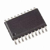
ATTINY26L-8SI Atmel, ATTINY26L-8SI Datasheet - Page 97

ATTINY26L-8SI
Manufacturer Part Number
ATTINY26L-8SI
Description
IC AVR MCU 2K LV 8MHZ IND 20SOIC
Manufacturer
Atmel
Series
AVR® ATtinyr
Specifications of ATTINY26L-8SI
Core Processor
AVR
Core Size
8-Bit
Speed
8MHz
Connectivity
USI
Peripherals
Brown-out Detect/Reset, POR, PWM, WDT
Number Of I /o
16
Program Memory Size
2KB (1K x 16)
Program Memory Type
FLASH
Eeprom Size
128 x 8
Ram Size
128 x 8
Voltage - Supply (vcc/vdd)
2.7 V ~ 5.5 V
Data Converters
A/D 11x10b
Oscillator Type
Internal
Operating Temperature
-40°C ~ 85°C
Package / Case
20-SOIC (7.5mm Width)
Lead Free Status / RoHS Status
Contains lead / RoHS non-compliant
Available stocks
Company
Part Number
Manufacturer
Quantity
Price
Part Number:
ATTINY26L-8SI
Manufacturer:
ATMEL/爱特梅尔
Quantity:
20 000
- Current page: 97 of 182
- Download datasheet (3Mb)
1477K–AVR–08/10
The ADC module contains a prescaler, which divides the system clock to an acceptable ADC
clock frequency.
The ADPS bits in ADCSR are used to generate a proper ADC clock input frequency from any
chip clock frequency above 100 kHz. The prescaler starts counting from the moment the ADC is
switched on by setting the ADEN bit in ADCSR. The prescaler keeps running for as long as the
ADEN bit is set, and is continuously reset when ADEN is low.
When initiating a conversion by setting the ADSC bit in ADCSR, the conversion starts at the fol-
lowing rising edge of the ADC clock cycle. If differential channels are selected, the conversion
will only start at every other rising edge of the ADC clock cycle after ADEN was set.
A normal conversion takes 13 ADC clock cycles. In certain situations, the ADC needs more
clock cycles to initialization and minimize offset errors. Extended conversions take 25 ADC clock
cycles and occur as the first conversion after the ADC is switched on (ADEN in ADCSR is set).
Special care should be taken when changing differential channels. Once a differential channel
has been selected, the gain stage may take as much as 125 µs to stabilize to the new value.
Thus conversions should not be started within the first 125 µs after selecting a new differential
channel. Alternatively, conversions results obtained within this period should be discarded. The
same settling time should be observed for the first differential conversion after changing ADC
reference (by changing the REFS1:0 bits in ADMUX).
The actual sample-and-hold takes place 1.5 ADC clock cycles after the start of a normal conver-
sion and 13.5 ADC clock cycles after the start of an extended conversion. When a conversion is
complete, the result is written to the ADC Data Registers, and ADIF is set. In Single Conversion
mode, ADSC is cleared simultaneously. The software may then set ADSC again, and a new
conversion will be initiated on the first rising ADC clock edge. In Free Running mode, a new con-
version will be started immediately after the conversion completes, while ADSC remains high.
Using Free Running mode and an ADC clock frequency of 200 kHz gives the lowest conversion
time, 65
Figure 53. ADC Timing Diagram, Extended Conversion (Single Conversion Mode)
Cycle Number
ADC Clock
ADEN
ADSC
ADIF
ADCH
ADCL
µs
, equivalent to 15 kSPS. For a summary of conversion times, see Table 43.
1
2
MUX and REFS
Update
12
13
14
15
Sample & Hold
16
Extended Conversion
17
18
19
20
21
22
Conversion
Complete
23
24
25
MSB of Result
LSB of Result
Next
Conversion
1
2
MUX and REFS
Update
3
97
Related parts for ATTINY26L-8SI
Image
Part Number
Description
Manufacturer
Datasheet
Request
R

Part Number:
Description:
Manufacturer:
Atmel Corporation
Datasheet:

Part Number:
Description:
IC AVR MCU 2K 16MHZ IND 32-QFN
Manufacturer:
Atmel
Datasheet:

Part Number:
Description:
IC AVR MCU 2K 16MHZ IND 20-SOIC
Manufacturer:
Atmel
Datasheet:

Part Number:
Description:
IC AVR MCU 2K 16MHZ IND 20-DIP
Manufacturer:
Atmel
Datasheet:

Part Number:
Description:
IC AVR MCU 2K 16MHZ IND 32-QFN
Manufacturer:
Atmel
Datasheet:

Part Number:
Description:
IC AVR MCU 2K 16MHZ IND 20-DIP
Manufacturer:
Atmel
Datasheet:

Part Number:
Description:
IC AVR MCU 2K 16MHZ COM 20-SOIC
Manufacturer:
Atmel
Datasheet:

Part Number:
Description:
IC AVR MCU 2K 16MHZ IND 20-SOIC
Manufacturer:
Atmel
Datasheet:

Part Number:
Description:
ID MCU AVR 2K 5V 16MHZ 32-QFN
Manufacturer:
Atmel
Datasheet:

Part Number:
Description:
Microcontrollers (MCU) AVR 2K FLASH 128B EE 128B SRAM ADC
Manufacturer:
Atmel
Datasheet:

Part Number:
Description:
IC AVR MCU 2K 16MHZ COM 32-QFN
Manufacturer:
Atmel
Datasheet:

Part Number:
Description:
IC AVR MCU 2K 16MHZ COM 20-DIP
Manufacturer:
Atmel
Datasheet:

Part Number:
Description:
ID MCU AVR 2K 5V 16MHZ 20-DIP
Manufacturer:
Atmel
Datasheet:

Part Number:
Description:
ID MCU AVR 2K 5V 16MHZ 20-SOIC
Manufacturer:
Atmel
Datasheet:


