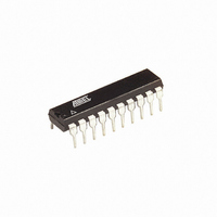
AT89LP4052-16PI Atmel, AT89LP4052-16PI Datasheet - Page 59

AT89LP4052-16PI
Manufacturer Part Number
AT89LP4052-16PI
Description
IC 8051 MCU FLASH 4K 20DIP
Manufacturer
Atmel
Series
89LPr
Datasheet
1.AT89LP2052-20PU.pdf
(94 pages)
Specifications of AT89LP4052-16PI
Core Processor
8051
Core Size
8-Bit
Speed
16MHz
Connectivity
SPI, UART/USART
Peripherals
Brown-out Detect/Reset, POR, PWM, WDT
Number Of I /o
15
Program Memory Size
4KB (4K x 8)
Program Memory Type
FLASH
Ram Size
256 x 8
Voltage - Supply (vcc/vdd)
2.4 V ~ 5.5 V
Oscillator Type
Internal
Operating Temperature
-40°C ~ 85°C
Package / Case
20-DIP (0.300", 7.62mm)
Lead Free Status / RoHS Status
Contains lead / RoHS non-compliant
Eeprom Size
-
Data Converters
-
Other names
AT89LP4052-20PI
AT89LP4052-20PI
AT89LP4052-20PI
Available stocks
Company
Part Number
Manufacturer
Quantity
Price
Company:
Part Number:
AT89LP4052-16PI
Manufacturer:
ITT
Quantity:
10
23.2
Table 23-2.
23.3
23.4
3547J–MICRO–10/09
Symbol
LOAD
SUCCESS
WRTINH
BUSY
Bit
Status Register
DATA Polling
Parallel Programming
Function
Load flag. Cleared low by the load page buffer command and set high by the next memory write. This flag signals that
the page buffer was previously loaded with data by the load page buffer command.
Success flag. Cleared low at the start of a programming cycle and will only be set high if the programming cycle
completes without interruption from the brownout detector.
Write Inhibit flag. Cleared low by the brownout detector (BOD) whenever programming is inhibited due to V
below the minimum required programming voltage. If a BOD episode occurs during programming, the SUCCESS flag
will remain low after the cycle is complete. WRTINH low also forces BUSY low.
Busy flag. Cleared low whenever the memory is busy programming or if write is currently inhibited.
Status
–
7
Register
The current state of the memory may be accessed by reading the status register. The status reg-
ister is shown in
The AT89LP2052/LP4052 implements DATA polling to indicate the end of a programming cycle.
While the device is busy, any attempted read of the last byte written will return the data byte with
the MSB complemented. Once the programming cycle has completed, the true value will be
accessible. During Erase the data is assumed to be FFH and DATA polling will return 7FH.
When writing multiple bytes in a page, the DATA value will be the last data byte loaded before
programming begins, not the written byte with the highest physical address within the page.
Parallel Programming Mode is enabled by applying V
required during parallel mode are shown in
configured as an 8-bit wide bidirectional command bus. Data on P1 is strobed by a positive
pulse on the XTAL1 pin. No other clock is required. The interface is enabled by pulling CS (P3.2)
low. P3.1 acts as RDY/BSY, and will be pulled low to indicate that the device is busy regardless
of the state of CS.
–
6
Table
–
5
23-2.
–
4
LOAD
Figure
3
23-2. During parallel programming, Port 1 is
SUCCESS
AT89LP2052/LP4052
2
PP
to the RST pin. The connections
WRTINH
1
BUSY
0
CC
falling
59


