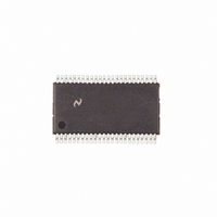
COP8SCE9IMT9 National Semiconductor, COP8SCE9IMT9 Datasheet - Page 22

COP8SCE9IMT9
Manufacturer Part Number
COP8SCE9IMT9
Description
IC MCU EEPROM 8BIT 8K 48-TSSOP
Manufacturer
National Semiconductor
Series
COP8™ 8Sr
Datasheet
1.COP8SDE9IMT9NOPB.pdf
(70 pages)
Specifications of COP8SCE9IMT9
Core Processor
COP8
Core Size
8-Bit
Speed
20MHz
Connectivity
Microwire/Plus (SPI), UART/USART
Peripherals
Brown-out Detect/Reset, POR, PWM, WDT
Number Of I /o
39
Program Memory Size
8KB (8K x 8)
Program Memory Type
FLASH
Ram Size
256 x 8
Voltage - Supply (vcc/vdd)
2.7 V ~ 5.5 V
Oscillator Type
Internal
Operating Temperature
0°C ~ 70°C
Package / Case
48-TSSOP
Lead Free Status / RoHS Status
Contains lead / RoHS non-compliant
Eeprom Size
-
Data Converters
-
Other names
*COP8SCE9IMT9
www.national.com
5.0 In-System Programming
power-up executing from Boot ROM. When FLEX = 0, this
assumes that either the MICROWIRE/PLUS ISP routine or
external programming is being used to program the device. If
using the MICROWIRE/PLUS ISP routine, the software in
the boot ROM will monitor the MICROWIRE/PLUS for com-
mands to program the flash memory. When programming
the flash program memory is complete, the FLEX bit will
have to be programmed to a 1 and the device will have to be
reset, either by pulling external Reset to ground or by a
MICROWIRE/PLUS ISP EXIT command, before execution
from flash program memory will occur.
If FLEX = 1, upon exiting Reset, the device will begin ex-
ecuting from location 0000 in the flash program memory. The
assumption, here, is that either the application is not using
ISP, is using MICROWIRE/PLUS ISP by jumping to it within
the application code, or is using a customized ISP routine. If
a customized ISP routine is being used, then it must be
programmed into the flash memory by means of the
MICROWIRE/PLUS ISP or external programming as de-
scribed in the preceding paragraph.
5.3 REGISTERS
There are six registers required to support ISP: Address
Register Hi byte (ISPADHI), Address Register Low byte
(ISPADLO), Read Data Register (ISPRD), Write Data Reg-
ister (ISPWR), Write Timing Register (PGMTIM), and the
Control Register (ISPCNTRL). The ISPCNTRL Register is
not available to the user.
5.3.1 ISP Address Registers
The address registers (ISPADHI & ISPADLO) are used to
specify the address of the byte of data being written or read.
For page erase operations, the address of the beginning of
the page should be loaded. For mass erase operations,
0000 must be placed into the address registers. When read-
ing the Option register, FFFF (hex) should be placed into the
address registers. Registers ISPADHI and ISPADLO are
cleared to 00 on Reset. These registers can be loaded from
either flash program memory or Boot ROM and must be
maintained for the entire duration of the operation.
Note: The actual memory address of the Option Register is
0x3FFF (hex), however the MICROWIRE/PLUS ISP routines
require the address FFFF (hex) to be used to read the
Option Register when the Flash Memory is secured.
(Continued)
Addr 15 Addr 14
Bit 7
7
0
0
0
0
0
Bit 6
TABLE 5. High Byte of ISP Address
6
0
0
0
0
0
Addr 13
Bit 5
Addr 12 Addr 11 Addr 10
Bit 4
ISPADHi
5
0
0
0
0
0
Bit 3
Bit 2
4
0
0
0
0
0
Register Bit
TABLE 9. PGMTIM Register Format
Addr 9
Bit 1
3
0
0
0
0
0
Addr 8
Bit 0
PGMTIM
22
2
0
0
0
1
1
5.3.2 ISP Read Data Register
The Read Data Register (ISPRD) contains the value read
back from a read operation. This register can be accessed
from either flash program memory or Boot ROM. This regis-
ter is undefined on Reset.
5.3.3 ISP Write Data Register
The Write Data Register (ISPWR) contains the data to be
written into the specified address. This register is undeter-
mined on Reset. This register can be accessed from either
flash program memory or Boot ROM. The Write Data register
must be maintained for the entire duration of the operation.
5.3.4 ISP Write Timing Register
The Write Timing Register (PGMTIM) is used to control the
width of the timing pulses for write and erase operations. The
value to be written into this register is dependent on the
frequency of CKI and is shown in Table 9 . This register must
be written before any write or erase operation can take
place. It only needs to be loaded once, for each value of CKI
frequency. This register can be loaded from either flash
program memory or Boot ROM and must be maintained for
the entire duration of the operation. The MICROWIRE/PLUS
ISP routine that is resident in the boot ROM requires that this
Register be defined prior to any access to the Flash memory.
Refer to 5.7 MICROWIRE/PLUS ISP for more information on
available ISP commands. On Reset, the PGMTIM register is
loaded with the value that corresponds to 10 MHz frequency
for CKI.
Bit 7
Bit 7
Addr 7
Bit7
Bit7
Bit 7
Bit 6
Bit 6
Bit6
Bit6
1
0
1
1
0
0
Addr 6
Bit 6
TABLE 6. Low Byte of ISP Address
TABLE 8. ISP Write Data Register
TABLE 7. ISP Read Data Register
Bit 5
Bit 5
Addr 5
Bit5
Bit5
Bit 5
0
1
0
1
0
1
Addr 4
Bit 4
Bit 4
Bit 4
Bit4
Bit4
ISPADLO
ISPWR
ISPRD
Addr 3
Bit 3
Bit 3
Bit3
Bit3
Bit 3
CKI Frequency Range
62.5 kHz–83.3 kHz
50 kHz–66.67 kHz
25 kHz–33.3 kHz
37.5 kHz–50 kHz
75 kHz–100 kHz
Bit 2
Bit 2
Addr 2
Bit2
Bit2
Bit 2
Addr 1
Bit 1
Bit 1
Bit 1
Bit1
Bit1
Addr 0
Bit 0
Bit 0
Bit 0
Bit0
Bit0


