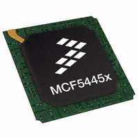
MCF54452VR266 Freescale Semiconductor, MCF54452VR266 Datasheet - Page 40

MCF54452VR266
Manufacturer Part Number
MCF54452VR266
Description
IC MPU 32BIT 266MHZ 360TEPBGA
Manufacturer
Freescale Semiconductor
Series
MCF5445xr
Datasheet
1.MCF54452CVR200.pdf
(48 pages)
Specifications of MCF54452VR266
Core Processor
Coldfire V4
Core Size
32-Bit
Speed
266MHz
Connectivity
I²C, SPI, SSI, UART/USART, USB OTG
Peripherals
DMA, WDT
Number Of I /o
132
Program Memory Type
ROMless
Ram Size
32K x 8
Voltage - Supply (vcc/vdd)
1.35 V ~ 3.6 V
Oscillator Type
Internal
Operating Temperature
0°C ~ 70°C
Package / Case
360-TEPBGA
Family Name
MCF5445X
Device Core
ColdFire
Device Core Size
32b
Frequency (max)
266MHz
Instruction Set Architecture
RISC
Supply Voltage 1 (typ)
3.3V
Operating Supply Voltage (max)
1.65/3.6V
Operating Supply Voltage (min)
1.35/3V
Operating Temp Range
0C to 70C
Operating Temperature Classification
Commercial
Mounting
Surface Mount
Pin Count
360
Package Type
TEBGA
Leaded Process Compatible
Yes
Rohs Compliant
Yes
Peak Reflow Compatible (260 C)
Yes
For Use With
M54455EVB - BOARD EVAL FOR MCF5445X
Lead Free Status / RoHS Status
Lead free / RoHS Compliant
Eeprom Size
-
Program Memory Size
-
Data Converters
-
Lead Free Status / Rohs Status
Compliant
Available stocks
Company
Part Number
Manufacturer
Quantity
Price
Company:
Part Number:
MCF54452VR266
Manufacturer:
Freescale Semiconductor
Quantity:
135
Company:
Part Number:
MCF54452VR266
Manufacturer:
FREESCAL
Quantity:
329
Electrical Characteristics
5.19
40
1
Num
JTAG and Boundary Scan Timing
J10
J11
J12
J13
J14
JTAG_EN is expected to be a static signal. Hence, specific timing is not associated with it.
J1
J2
J3
J4
J5
J6
J7
J8
J9
TCLK
(input)
TCLK Frequency of Operation
TCLK Cycle Period
TCLK Clock Pulse Width
TCLK Rise and Fall Times
Boundary Scan Input Data Setup Time to TCLK Rise
Boundary Scan Input Data Hold Time after TCLK Rise
TCLK Low to Boundary Scan Output Data Valid
TCLK Low to Boundary Scan Output High Z
TMS, TDI Input Data Setup Time to TCLK Rise
TMS, TDI Input Data Hold Time after TCLK Rise
TCLK Low to TDO Data Valid
TCLK Low to TDO High Z
TRST Assert Time
TRST Setup Time (Negation) to TCLK High
J4
MCF5445x ColdFire
V
IH
Table 29. JTAG and Boundary Scan Timing
Characteristics
V
IL
Figure 27. Test Clock Input Timing
J3
®
Microprocessor Data Sheet, Rev. 6
1
J4
J2
J3
Min
DC
50
20
20
10
50
10
—
—
—
—
—
5
4
Max
20
30
33
33
11
11
—
—
—
—
—
—
—
3
Freescale Semiconductor
MHz
Unit
ns
ns
ns
ns
ns
ns
ns
ns
ns
ns
ns
ns
ns


