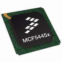
MCF54453VR266 Freescale Semiconductor, MCF54453VR266 Datasheet - Page 7

MCF54453VR266
Manufacturer Part Number
MCF54453VR266
Description
IC MPU 32BIT 266MHZ 360TEPBGA
Manufacturer
Freescale Semiconductor
Series
MCF5445xr
Datasheet
1.MCF54452CVR200.pdf
(48 pages)
Specifications of MCF54453VR266
Core Processor
Coldfire V4
Core Size
32-Bit
Speed
266MHz
Connectivity
I²C, SPI, SSI, UART/USART, USB OTG
Peripherals
DMA, WDT
Number Of I /o
132
Program Memory Type
ROMless
Ram Size
32K x 8
Voltage - Supply (vcc/vdd)
1.35 V ~ 3.6 V
Oscillator Type
Internal
Operating Temperature
0°C ~ 70°C
Package / Case
360-TEPBGA
Processor Series
MCF544x
Core
ColdFire V4
Data Bus Width
32 bit
Program Memory Size
16 KB
Data Ram Size
32 KB
Interface Type
I2C, SPI, SSI
Maximum Clock Frequency
66 MHz
Number Of Timers
8
Operating Supply Voltage
- 0.3 V to + 4 V
Maximum Operating Temperature
+ 70 C
Mounting Style
SMD/SMT
3rd Party Development Tools
JLINK-CF-BDM26, EWCF
Development Tools By Supplier
M54455EVB
Minimum Operating Temperature
0 C
On-chip Adc
16 bit, 16 Channel
On-chip Dac
16 bit, 16 Channel
For Use With
M54455EVB - BOARD EVAL FOR MCF5445X
Lead Free Status / RoHS Status
Lead free / RoHS Compliant
Eeprom Size
-
Program Memory Size
-
Data Converters
-
Lead Free Status / Rohs Status
Lead free / RoHS Compliant
Available stocks
Company
Part Number
Manufacturer
Quantity
Price
Company:
Part Number:
MCF54453VR266
Manufacturer:
Freescale Semiconductor
Quantity:
135
3.3.1
If EV
to the EV
must power up. The rise times on the power supplies should be slower than 50 V/millisecond to avoid turning on the internal
ESD protection clamp diodes.
3.3.2
If IV
There is no limit on how long after IV
requirements for the fall times of the power supplies.
4
4.1
The following table lists all the MCF5445x pins grouped by function. The Dir column is the direction for the primary function
of the pin only. Refer to
of the MCF5445x signals, consult the MCF54455 Reference Manual (MCF54455RM).
Freescale Semiconductor
DD
DD
/PV
/SDV
DD
DD
Pin Assignments and Reset States
Signal Multiplexing
/SDV
DD
Power-Up Sequence
Power-Down Sequence
are powered down first, sense circuits in the I/O pads cause all output drivers to be in a high impedance state.
are powered up with the IV
DD
In this table and throughout this document, a single signal within a group is designated
without square brackets (i.e., FB_AD23), while designations for multiple signals within a
group use brackets (i.e., FB_AD[23:21]) and is meant to include all signals within the two
bracketed numbers when these numbers are separated by a colon.
The primary functionality of a pin is not necessarily its default functionality. Most pins that
are muxed with GPIO default to their GPIO functionality. See
exceptions.
to be in a high impedance state. There is no limit on how long after EV
Section 4, “Pin Assignments and Reset
FB_BE/BWE[3:0]
FB_AD[31:0]
FB_CS[3:1]
FB_R/W
FB_OE
FB_TS
FB_TA
MCF5445x ColdFire
Table 3. Special-Case Default Signal Functionality
Pin
DD
and PV
DD
FB_AD[31:0] except when serial boot selects 0-bit
at 0 V, the sense circuits in the I/O pads cause all pad output drivers connected
DD
256 MAPBGA
power down before EV
®
Microprocessor Data Sheet, Rev. 6
NOTE
NOTE
FB_BE/BWE[3:0]
States,”
boot port size.
FB_CS[3:1]
FB_R/W
FB_OE
FB_TS
FB_TA
for package diagrams. For a more detailed discussion
DD
360 TEPBGA
or SDV
Table 3
DD
for a list of the
Pin Assignments and Reset States
DD
must power down. There are no
/SDV
DD
powers up before IV
DD
7


