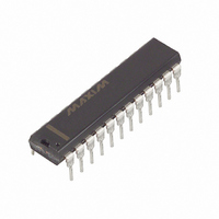
MAXQ3210-EMX+ Maxim Integrated Products, MAXQ3210-EMX+ Datasheet - Page 2

MAXQ3210-EMX+
Manufacturer Part Number
MAXQ3210-EMX+
Description
IC MCU 16BIT LP 24-DIP
Manufacturer
Maxim Integrated Products
Series
MAXQ™r
Datasheet
1.MAXQ3210-EJX.pdf
(28 pages)
Specifications of MAXQ3210-EMX+
Core Processor
RISC
Core Size
16-Bit
Speed
3.6MHz
Peripherals
LED, Power-Fail Reset, POR, PWM, WDT
Number Of I /o
15
Program Memory Size
2KB (1K x 16)
Program Memory Type
EEPROM
Eeprom Size
128 x 8
Ram Size
64 x 8
Voltage - Supply (vcc/vdd)
4.5 V ~ 5.5 V
Oscillator Type
Internal
Operating Temperature
-40°C ~ 85°C
Package / Case
24-DIP (0.300", 7.62mm)
Processor Series
MAXQ3210
Core
RISC
Data Bus Width
16 bit
Data Ram Size
64 B
Interface Type
JTAG
Maximum Clock Frequency
3.58 mhZ
Number Of Programmable I/os
15
Number Of Timers
1
Operating Supply Voltage
6 V to 9.5 V
Maximum Operating Temperature
+ 85 C
Mounting Style
SMD/SMT
Development Tools By Supplier
MAXQ3210-KIT
Minimum Operating Temperature
- 40 C
Lead Free Status / RoHS Status
Lead free / RoHS Compliant
Data Converters
-
Connectivity
-
Lead Free Status / Rohs Status
Details
Voltage Range on Any Digital I/O Pin
Voltage Range on Any Analog I/O Pin
Voltage Range on V
Voltage Range on FEED Relative to Ground..........-0.5V to +20V
Microcontroller with Internal Voltage Regulator,
Piezoelectric Horn Driver, and Comparator
ABSOLUTE MAXIMUM RATINGS
ELECTRICAL CHARACTERISTICS
(V
Stresses beyond those listed under “Absolute Maximum Ratings” may cause permanent damage to the device. These are stress ratings only, and functional
operation of the device at these or any other conditions beyond those indicated in the operational sections of the specifications is not implied. Exposure to
absolute maximum rating conditions for extended periods may affect device reliability.
2
Supply Voltage
Internal Regulated Supply
Voltage
Voltage Regulator Output
Low-Battery Detection Threshold
Power-Fail Reset
Active Current
Stop-Mode Current
RESET Pullup
Relative to Ground
Relative to Ground..............................-0.5V to (V
DD
_____________________________________________________________________
= V
DD(MIN)
PARAMETER
to V
DD
...................................
DD(MAX)
Relative to Ground .........-0.5V to +10.5V
, C
REGOUT
SYMBOL
V
V
-0.5V to (V
REGOUT
I
I
I
= 10µF + 0.1µF, C
STOP1
STOP2
STOP3
V
R
I
I
I
I
I
I
V
DDINT
V
DD1
DD2
DD3
DD4
DD5
DD6
RST
RST
DD
BF
DDINT
DDINT
Maximum I
0°C to +85°C
-40°C
/1 mode (Note 2)
sysclk = f
/2 mode (Note 2)
sysclk = f
/4 mode (Note 2)
sysclk = f
/8 mode (Note 2)
sysclk = f
PMM1 mode (Note 2)
sysclk = f
8kHz ring mode (Note 2)
Brownout detector off, wake-up timer on,
T
Brownout detector off, wake-up timer on,
T
Brownout detector on, wake-up timer on,
T
V
A
A
A
RST
= +50°C (Note 3), V
= +25°C, V
= +25°C, V
= 0.4V, V
+ 0.5V)
+ 0.5V)
VDD
HFXIN
HFXIN
HFXIN
HFXIN
HFXIN
SOURCE
= 1µF, T
DD
DD
REGOUT
CONDITIONS
/ 2
/ 4
/ 8
/ 256
= 9V
= 9V
= 50mA
Continuous Output Current (any single I/O pin) .................25mA
Continuous Output Current (all I/O pins combined) ...........25mA
Operating Temperature Range ...........................-40°C to +85°C
Storage Temperature Range .............................-65°C to +150°C
Soldering Temperature .......................................See IPC/JEDEC
A
= -40°C to +85°C. Typical values are at T
DD
= 5.5V
= 9V
MIN
4.15
102
6.0
4.5
4.5
7.0
6.9
TYP
150
9.0
5.0
5.0
6.4
4.0
2.9
2.3
1.7
0.6
7.5
5.5
51
J-STD-020 Specification
A
= +25°C.) (Note 1)
MAX
7.51
33.0
250
9.5
5.5
5.5
7.6
4.6
9.0
6.0
4.5
3.5
3.0
1.2
13
80
UNITS
mA
mA
mA
mA
mA
mA
kΩ
µA
V
V
V
V
V


