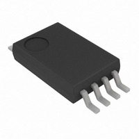
MCP602-I/ST Microchip Technology, MCP602-I/ST Datasheet - Page 2

MCP602-I/ST
Manufacturer Part Number
MCP602-I/ST
Description
IC OPAMP DUAL SNGL SUPPLY 8TSSOP
Manufacturer
Microchip Technology
Datasheet
1.MCP601T-IOT.pdf
(34 pages)
Specifications of MCP602-I/ST
Slew Rate
2.3 V/µs
Amplifier Type
General Purpose
Number Of Circuits
2
Output Type
Rail-to-Rail
Gain Bandwidth Product
2.8MHz
Current - Input Bias
1pA
Voltage - Input Offset
700µV
Current - Supply
230µA
Current - Output / Channel
22mA
Voltage - Supply, Single/dual (±)
2.7 V ~ 6 V
Operating Temperature
-40°C ~ 85°C
Mounting Type
Surface Mount
Package / Case
8-TSSOP
Op Amp Type
CMOS
No. Of Amplifiers
2
Bandwidth
2.8MHz
Supply Voltage Range
2.7V To 6V
Amplifier Case Style
TSSOP
No. Of Pins
8
Lead Free Status / RoHS Status
Contains lead / RoHS non-compliant
-3db Bandwidth
-
Lead Free Status / RoHS Status
Lead free / RoHS Compliant, Contains lead / RoHS non-compliant
Available stocks
Company
Part Number
Manufacturer
Quantity
Price
Company:
Part Number:
MCP602-I/ST
Manufacturer:
Microchip
Quantity:
5 661
Part Number:
MCP602-I/ST
Manufacturer:
MICROCHIP/微芯
Quantity:
20 000
MCP601/1R/2/3/4
1.0
Absolute Maximum Ratings †
V
Current at Input Pins .....................................................±2 mA
Analog Inputs (V
All Other Inputs and Outputs ......... V
Difference Input Voltage ...................................... |V
Output Short Circuit Current .................................Continuous
Current at Output and Supply Pins ............................±30 mA
Storage Temperature....................................–65°C to +150°C
Maximum Junction Temperature (T
ESD Protection On All Pins (HBM; MM) .............. ≥ 3 kV; 200V
DC CHARACTERISTICS
DS21314G-page 2
Electrical Specifications: Unless otherwise specified, T
V
Input Offset
Input Offset Voltage
Input Offset Temperature Drift
Power Supply Rejection
Input Current and Impedance
Input Bias Current
Input Offset Current
Common Mode Input Impedance
Differential Input Impedance
Common Mode
Common Mode Input Range
Common Mode Rejection Ratio
Open-loop Gain
DC Open-loop Gain (large signal)
Output
Maximum Output Voltage Swing
Linear Output Voltage Swing
Output Short Circuit Current
Power Supply
Supply Voltage
Quiescent Current per Amplifier
Note 1:
DD
OUT
Industrial Temperature
Extended Temperature
Industrial Temperature
Extended Temperature
– V
≈ V
2:
SS
ELECTRICAL
CHARACTERISTICS
DD
........................................................................7.0V
Parameters
/2, V
These specifications are not tested in either the SOT-23 or TSSOP packages with date codes older than YYWW = 0408.
In these cases, the minimum and maximum values are by design and characterization only.
All parts with date codes November 2007 and later have been screened to ensure operation at V
other minimum and maximum specifications are measured at 1.4V and/or 5.5V.
IN
L
+, V
= V
IN
DD
–) †† ........ V
/2, and R
L
J
) ......................... .+150°C
= 100 kΩ to V
ΔV
V
V
SS
SS
CMRR
OL
OL
PSRR
Z
V
V
V
Sym
V
V
V
OS
Z
A
A
V
– 1.0V to V
– 0.3V to V
I
I
I
DIFF
CMR
OUT
OUT
OS
SC
SC
I
I
I
I
, V
, V
CM
OS
OS
OS
OL
OL
DD
B
B
B
Q
/ΔT
OH
OH
A
V
V
V
V
V
L
SS
SS
SS
SS
SS
, and CS is tied low. (Refer to
DD
DD
DD
Min
-4.5
100
2.7
—
80
—
—
—
—
—
—
75
95
—
—
—
-2
-3
+ 100
+ 100
– 0.3
+ 15
+ 45
+ 1.0V
+ 0.3V
– V
A
SS
= +25°C, V
10
10
|
±0.7
±2.5
Typ
450
115
110
±22
±12
230
±1
±1
88
20
±1
—
90
—
—
—
—
—
13
13
1
||6
||3
V
V
V
V
V
DD
DD
DD
DD
DD
DD
5000
† Notice: Stresses above those listed under “Absolute
Maximum Ratings” may cause permanent damage to the
device. This is a stress rating only and functional operation of
the device at those or any other conditions above those
indicated in the operational listings of this specification is not
implied. Exposure to maximum rating conditions for extended
periods may affect device reliability.
†† See Section 4.1.2 “Input Voltage and Current Limits”.
+4.5
Max
325
6.0
+2
+3
60
—
—
—
—
—
—
—
—
—
—
—
– 100
– 100
– 1.2
= +2.7V to +5.5V, V
– 20
– 60
Figure 1-2
µV/°C T
Units
Ω||pF
Ω||pF
mV
mV
mV
mV
mV
mV
mV
mA
mA
dB
pA
pA
pA
pA
dB
dB
dB
µA
V
V
V
V
T
T
T
T
R
V
R
V
R
R
R
R
V
V
(Note 2)
I
O
A
A
A
A
A
DD
DD
OUT
OUT
DD
DD
L
L
L
L
L
L
= 0
and
= -40°C to +85°C (Note 1)
= -40°C to +125°C (Note 1)
= -40°C to +125°C
= +85°C (Note 1)
= +125°C (Note 1)
= 25 kΩ to V
= 5 kΩ to V
= 25 kΩ to V
= 5 kΩ to V
= 25 kΩ to V
= 5 kΩ to V
= 2.7V to 5.5V
= 5.0V, V
= 5.5V
= 2.7V
SS
= 0.1V to V
= 0.1V to V
Figure
= GND, V
© 2007 Microchip Technology Inc.
CM
1-3).
L
L
L
,
, Output overdrive = 0.5V
, A
L
L
L
Conditions
,
, Output overdrive = 0.5V
, A
DD
DD
= -0.3V to 3.8V
CM
OL
OL
– 0.1V
– 0.1V
DD
= V
≥ 95 dB
≥ 100 dB
=6.0V. However, the
DD
/2,


